“Motor drive is a general term for micro motors or springs and accessories assembled in film cameras. The film is automatically rewinded with the help of micro motors. Most of them refer to 35 mm single-lens reflex cameras.
“
Motor drive Motor drive is a general term for micro motors or springs and their accessories assembled in film cameras. The film is automatically rewinded with the help of micro motors. Most of them refer to 35 mm single-lens reflex cameras.
01 Principle of power supply circuit
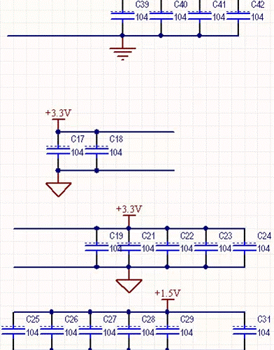
The schematic diagram of the power supply part is shown in Figure 1-1:

Picture 1-1
From Figure 1-1, we can see that there are three power supplies: +5V, +3.3V, and +1.5V. Each power supply has a 0.1µF bypass capacitor to bypass high-frequency crosstalk in the power supply to the ground to prevent high Frequency signals are crosstalked to other modules through the power supply. At the same time, the power frequency interference of the power supply itself can be filtered out.
It is worth noting that when wiring, the power output point after decoupling by the decoupling capacitor should be as close as possible to the power supply pin of the chip for power supply. The long lead may become an interference receiving antenna again, resulting in the decoupling effect. disappear. If it is not possible to make each power output point after decoupling close to the power pin of the chip, then you can use the method of decoupling separately, that is, connect the decoupling capacitor as close to the power pin of each chip as possible. It also explains why the 3.3V power supply in Figure 1-1 has two decoupling output points.
02. Principle of motor drive circuit
The principle of the motor drive circuit is shown in Figure 2-1:
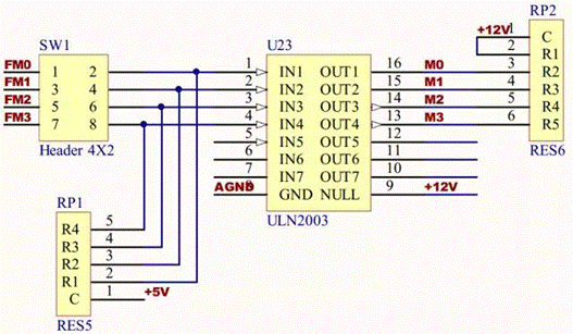
Figure 2-1
Header 4X2 in Figure 2-1 is 4 rows and 2 columns of pins, FM0~3 are FPGA chip I/O output ports, the added pins give a movable mechanism, and only use jumper caps to connect when needed. Improve the efficiency of I/O port usage. RES5 is a five-port exclusion resistor. It integrates 4 resistors with equal resistance and one end publicly connected. PIN 1 is the common end, and PIN2~5 are the output terminals of the exclusion. The exclusion principle diagram is shown in Figure 2-2:

Figure 2-2
The common terminal of the exclusion resistor is connected to the power supply, that is, in the form of a pull-up resistor. The function is to enhance the driving ability of the FPGA chip I/O port (hereinafter referred to as the I/O port). In fact, it is to increase the output current when the I/O output is high. . When the I/O output is high, the +5V power supply is connected to IN1~4 through the exclusion, which is equivalent to providing an additional current output source for the I/O, thereby improving the driving capability. When I/O outputs low level, I/O can be regarded as grounding, and because IN1~4 are directly connected with I/O by wires, they directly receive the low level output signal of I/O. At this time, the +5V power supply is grounded after the resistance R and the internal circuit of the I/O (resistance is approximately zero), so the current of this circuit cannot be greater than the maximum current (Ii) of the I/O. Formula 2-1:

The value range of exclusion can be obtained by formula 2-2.
In addition to improving the driving capability, the pull-up resistor has another function, which is to perform level conversion. After investigation, the interface logic of ULN2003 is: 5V-TTL, 5V-CMOS logic. In the case of 3.3V power supply, the I/O port can provide 3.3V-LVTTL, 3.3V-LVCMOS, 3.3V-PCI and SSTL-3 interface logic levels. Therefore, an external 5V pull-up resistor is needed to change the I/O level specification to 5V level logic.
The chip ULN2003 integrates 7 groups of Darlington tubes, which are specially used to increase the driving current. The logic between the chip pins is shown in Figure 2-3:

Figure 2-3

Figure 2-4
Since the I/O current is far from enough to drive the motor, it is necessary to connect the chip to drive the motor. The Darlington circuit integrated in ULN2003 is shown in Figure 2-4. The form of Darlington tube has the characteristic of transforming weak signal into strong electric signal. I/O level logic is input from PIN IN, and the strong electric signal input from PIN 9 (COMMON) terminal is controlled by Darlington tube according to I/O The signal changes regularly. It is worth noting that: ULN2003 output logic will be opposite to the input logic, this feature should be paid attention to when programming.
RES6 is a six-port exclusion resistor. It integrates five equal resistance resistors with one end connected in common. PIN 1 is the common end, and PIN2~6 are the output ends of the exclusion. For the schematic diagram and connection description, please refer to Figure 2- above. 2. For the calculation of the exclusion value range, please refer to formula 2-2, which will not be repeated here. It is worth noting that PIN 1 of RES6 is connected to PIN 2 because there is an unused resistor. In order to avoid PIN 2 from floating, PIN 2 is connected to PIN 1 (common terminal), which is the resistor corresponding to PIN 2. The pin that is short-circuited, which is not only avoided, but also makes the resistance invalid.
03 Principle of Motor Indicator Circuit
The motor indicator circuit is shown in Figure 3-1:

Figure 3-1
The indicator lights of the motor part are used to indicate the logic level status of each signal, among which R106~109 are current-limiting resistors to prevent the light-emitting diodes from being burnt due to excessive current. It is worth noting that the LEDs of this indicator are connected to a common anode, and the corresponding diodes are generated by the M0~3 signal port. The logic level of OUT and IN of ULN2003 is opposite. ~3 For example, output high level can light up the corresponding LED, for example: FM0 output high level, corresponding to LD17 light up, you should pay attention to this circuit inverting the actual logic of I/O twice during programming. The corresponding relationship is which high level output from the I/O port corresponds to which indicator light is lit.
04 Clock circuit principle
The clock circuit is shown in Figure 4-1:
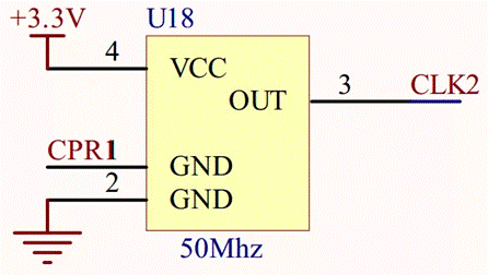
Pic 4-1
A 50Mhz active crystal oscillator is used to generate the clock signal. The connection method adopts the typical connection method of the active crystal oscillator: PIN 1 is suspended, PIN 2 is grounded, PIN 3 outputs the clock signal, and PIN 4 is connected to the power supply. Since the FPGA’s I/O power supply is 3.3V, and the clock signal generated by the clock circuit must be received by the I/O port, the maximum value of the clock signal cannot exceed 3.3V, so the clock circuit power supply adopts 3.3V power supply.
05FPGA part of the circuit principle
The schematic diagram of part of the FPGA circuit is shown in Figure 5-1:

Figure 5-1
Header 18X2 is an array of 18 rows and 2 rows. The two groups of rows are connected to PIN port, 3.3V power supply, and digital ground respectively. It provides a movable mechanism so that the PIN port can be connected to the target with a flat cable as needed to achieve signal transmission. the goal of. The 3.3V power supply and digital ground pin can be used to provide a logic high or logic low level for the target according to needs.
U21D is the clock signal receiving part of the FPGA chip, which is connected to the corresponding clock signal port through the network label “CLK0~3”.
U21C is the power supply and grounding part of the FPGA chip. The port that contains the word “GND” is the “ground” port, which is connected to the digital ground. VCCIO1~4 are the power supply ports of the I/O ports. They are powered by a 3.3V power supply and pass the network label “+3.3″. V” is connected to the 3.3V power port. VCCA_PLL1, VCCA_PLL2, and VCCINT are the power supply ports of the internal arithmetic unit and input buffer. They are powered by a 1.5V power supply and are connected to the 1.5V power supply port through the network label “+1.5V”.
U21B is the JTAG and AS download part. TMS, TCK, TD1 and TD0 are the mode selection terminal, clock signal terminal, data input terminal, and data output terminal of the JATAG download mode, respectively. DATA0 is the data port downloaded by AS. The MSEL0, MSEL1, nCE, nCEO, CONF_DONE, nCONFIG, and nSTATUS ports are connected according to the typical connection. It is worth noting that both AS and JTAG communicate through the JTAG standard. AS download is generally to download POF to PROM (flash), and it can still be loaded after power-on. JTAG download is to download the sof file directly to the FPGA through the JTAG port , It is generally used for temporary debugging, and it will be lost when the power is off.
U22 is an electrically erasable ROM, which is used to store the data downloaded by AS, so that the FPGA program segment can be saved even when power is off. The DATA terminal is the data reading terminal, which is used to read the data in the ROM. DCLK is a clock port, used to receive clock signals for synchronous transmission. nCS is a chip select port, used to receive chip select signals to indicate communication with the chip. ASDI is the AS download data input terminal, which is used to receive AS download data. VCC and GND are power port and ground port, respectively, connected to 3.3V and digital ground respectively.
The Links: ESD7181MUT5G 2MBI100N-060
0 Comments for “A detailed explanation of power supply and motor drive principles and circuit analysis”