“The concept of SoC (system on a chip) has become increasingly popular, and with the rapid development of FPGA technology, a programmable system-on-chip (SoPC), as a special embedded microprocessor system, combines the advantages of SoC and FPGA, and has soft The functions of hardware in system programmability, can be cut, can be expanded, can be upgraded, has gradually become an emerging technology direction. The core of SoPC is the embedded microprocessor core implemented on FPGA. At present, there are mainly 32-bit soft core MicroBlaze of Xilinx, 32-bit PowerPC series processor hard core PowerPC 405, and Altera’s Nios series microprocessor soft core, etc. .
“
Author: Lin Zhenhua; Sheng Lei
The concept of SoC (system on a chip) has become increasingly popular, and with the rapid development of FPGA technology, a programmable system-on-chip (SoPC), as a special embedded microprocessor system, combines the advantages of SoC and FPGA, and has soft The functions of hardware in system programmability, can be cut, can be expanded, can be upgraded, has gradually become an emerging technology direction. The core of SoPC is the embedded microprocessor core implemented on FPGA. At present, there are mainly 32-bit soft core MicroBlaze of Xilinx, 32-bit PowerPC series processor hard core PowerPC 405, and Altera’s Nios series microprocessor soft core, etc. .
The system introduced in this paper is an Ethernet interface device based on VME bus with PowerPC 405 as microprocessor. It realizes real-time data exchange between VME system and external local area network through Ethernet and VME bus interface.
hardware development
The development adopts EDK7.1 (embedded development kit) and ISE7.1 tool software of Xilinx Company. The EDK toolkit integrates the hardware platform generator (Platgen), software platform generator (Libgen), simulation model generator (Simgen), software compiler (Mb-gcc/ppc-gcc) and software debugging tool (Mb-gdb) /ppc-gdb), etc., through the provided integrated development environment XPS, users can call all the above tools to complete the entire process of embedded system development.
First, generate the hardware system framework and add the required IP cores in the XPS interface environment. You can also directly write the hardware description file (.MHS file) with a text editor, and then call Platgen to generate the netlist file of the embedded processing system ( .NGC file); then set the system software configuration through the software description file (.MSS file) generated by the system or manually edited, and call Libgen to generate the driver layer and library. Although there are some useful functional modules and peripheral interface IP cores in EDK’s IP library, such as DCM (Digital Clock Manager), processor reset, PLB/OPB bus interface, external memory controller (EMC), UART, GPIO, interrupt controller, timer, etc., making full use of these resources can build a relatively complete embedded microprocessor system, but it is not enough for many embedded computer systems with special dedicated circuits. How to design the user-specific circuit into the EDK system, there are generally two methods. The first is to use the EDK project as a subsystem to generate the ISE project with Export to PorjNav in XPS, and then use the dedicated circuit and processor sub-system in ISE to generate the ISE project. After the system (system.vhd) is synthesized into the top-level HDL file (system_stub.vhd), the integrated wiring is completed in ISE, and finally the hardware .bit file is obtained by Import from PorjNav in XPS, and then you can go back to XPS to complete and apply the software compose, download and debug. The second method is to design the dedicated circuit as a user-defined IP Core, and then call it directly in the system to realize it. The custom IP Core is designed with HDL and must meet the EDK specification, such as special directory structure and processor peripheral definition file (.MPD), peripheral analysis definition file (.PAO), etc. If the custom IP Core is to have a software driver, the design must fully comply with the corresponding PLB or OPB bus interface specification. After completing the hardware and driver design, you can add an application software project to the XPS project and write the application software, and then call the compiler corresponding to the processor to compile and synthesize the .bit file generated by the hardware synthesis, and then download it to the target board. Debugging is ready.
The hardware block diagram of this system is shown in Figure 1. In this design, the Virtex-II Pro series FPGA chip XC2VP40 is used, and the program memory and data memory of the system are placed on the chip to be implemented by Block RAM. The processor clock is divided and then sent to the OPB bus as the bus clock, which reduces the bus speed of the slow peripherals and makes the system collocation more reasonable.
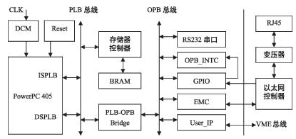
Figure 1 System hardware block diagram
PowerPC 405 is the core of this embedded system. It realizes fast access to program memory and data memory through PLB bus, and realizes on-chip OPB bus through PLB-OPB bridge, and then expands various peripherals through OPB bus. The OPB peripherals include an RS232 serial port, an OPB_EMC for expanding the Ethernet controller chip, a GPIO for the interrupt request of the Ethernet controller output, and an interrupt controller OPB_INTC to notify the PowerPC 405 of the external interrupt input by the GPIO and can set the priority. , and a user-defined IP Core is used to implement the interface circuit with the VME bus.
PowerPC 405 is a high-performance 32-bit PowerPC series processor core specially designed for embedded applications. For Virtex-II Pro series FPGA, its implementation model is PowerPC 405D5.
The PLB is a processor native bus that provides separate 32-bit address and 64-bit data buses for the instruction and data sides. The PLB bus architecture supports multiple master-slave devices. Each PLB master is connected to the PLB through an independent address bus, read data bus and write data bus. There is a central decision mechanism to authorize access to the PLB to allow the master to pass competition. to take ownership of the bus. OPB is an on-chip peripheral bus that provides a separate 32-bit address bus and 32-bit data bus, and is generally used to access low-speed and low-performance system resources. It is a fully synchronous bus, but not directly connected to the processor core, which accesses the OPB interface peripherals through the “PLB to OPB” bridge and the OPB bus.
The network controller adopts Cirrus Logic’s general-purpose single-chip 10/100M Ethernet controller CS8900A, which fully complies with the IEEE 802.3 Ethernet standard and supports complete full-duplex operation. Using EDK’s OPB_EMC IP can easily expand CS8900A as a device on the system OPB bus, as long as the address, data bus and control signal of the EMC port are connected to the address, data bus and control port of CS8900A respectively, and the EMC The timing parameters are set to be consistent with the requirements in the CS8900A manual. In addition, the interrupt output INTRQ of CS8900A is introduced into the system as a GPIO to realize the interrupt service function of Ethernet.
The content of the customized IP Core is shown in Figure 2. It uses the Block RAM resources in the FPGA to realize 64KB of dual-port RAM to complete the communication and data exchange with other devices on the VME bus. We use the second method above to embed the user-specific circuit into the microprocessor system. The custom IP mainly includes the OPB bus interface and the user circuit. We use the OPB bus IPIF template provided by EDK to modify it as Custom IP bus interface, 64KB dual-port RAM and VME bus interface are real user circuits.
Figure 2 Custom IP Core structure
software development
The embedded development environment EDK (Embedded Development Kit) divides software development into two parts, one is the development of the underlying system software, which mainly completes the functions of BSP (board support package); the other part is the development of user application software (including User hardware driver and user upper-layer application software). Since there are many IP cores and corresponding driver software in EDK, most of the development of the underlying system software can be completed with the help of the EDK integrated development environment, such as the selection of the operating system, the selection of device drivers, and interrupt/exception processing routines The settings of various system-level software parameters, including the settings of the operating system and the operating system parameters. The development of user application software has good portability due to the isolation of underlying drivers. The development and debugging of the entire user software can be completed in EDK.
● Low-level system software development
In this design, no operating system is used, and the so-called standalone mode is used, that is, EDK only provides hardware initialization and boot codes. In addition, it is necessary to generate low-level drivers for some peripherals such as GPIO, EMC, RS232, and interrupt controller. These can be set by selecting the dialog box of the menu Project->Software Platform Settings in the EDK integrated environment XPS, as shown in Figure 3. . Its essence is to automatically modify the .MSS file of the project. For example, the processing routine of the interrupt function can be set in the interface as shown in FIG. 4 . You can also manually edit the .MSS file to set the following settings:
PARAMETER int_handler = CS8900A_INT_HANDLER, int_port = IP2INTC_Irpt
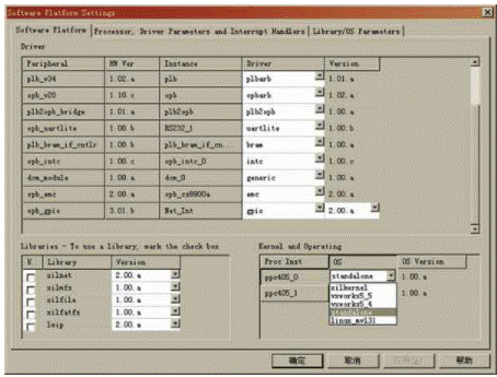
Figure 3 Setting up the operating system and drivers in XPS
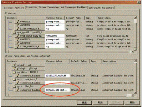
Figure 4 Setting up an interrupt service routine in XPS
After the setting is completed, run Tools->Generate Libraries and BSPs in XPS to call LibGen to automatically generate driver library files. The settings, operation function implementation or definition of these CPU and peripheral driver libraries can be implemented as processor instances in the project root directory. It is found in the corresponding subdirectories of each module under the libsrc directory under the directory named name, and referring to its implementation helps to deeply understand what actually happens. For example, the interrupt vector table can be found in the xintc_g.c file under the subdirectory of the mid-segment vector controller module (intc_v1_00_csrc in this example).
● User software development
For reading and writing mapped devices, the difference between these two I/O functions and *pDestMem = Value (direct read and write memory operations) is that the former performs read and write synchronization (calling the eieio assembly instruction). Refer to the chip manual to write the CS8900A driver to implement the basic I/O operations CS8900A_SendFrame and CS8900A_RecvFrame. There is a paid Ethernet IP CORE in EDK and some TCP/IP protocol stacks are attached. This protocol stack implements most common functions, but some important functions are not implemented. How interrupts work for operations. By modifying, adding and perfecting these software packages, a network programming interface that really faces higher-level application software for users is realized.
● Some problems in software development
Several main problems encountered in the software development process are summarized as follows:
(1) IEEE 802.3 network and network controller CS8900A all use Little Endian encoding, while the processor PowerPC 405D5 included in XC2VP40 uses Big Endian encoding, so it needs to be converted in the data I/O process.
(2) The linking process of the application program can be controlled by writing a linking control script file, thereby controlling the relocation process of the program image in the memory. This is sometimes useful in environments with limited memory resources such as FPGAs.
(3) The default bootloop program provided by EDK should be packaged into the hardware initialization stream. The purpose of this is to provide the default CPU reset to run the program to ensure that the CPU is in a predictable state, not because random randomness in the memory is executed. code in an unknown state.
System debugging method
Since the PowerPC 405 processor core already contains the debug module, which is exported by the JTAG port, as long as an IP module called JTAGPPC is added to the system and connected to the PowerPC 405, its debug port can be serialized into the JTAG chain of the FPGA, so that only Using the FPGA’s own download cable and JTAG interface can complete the system software debugging without adding additional circuits.
The software debugging tools provided by EDK mainly include XMD and GDB. It is worth mentioning that when using XMD to download the executable program image, the relocation of each program segment will also be displayed, and an error will be reported when an error occurs, such as the required address space is larger than the actual provided address space and other errors, and this is in EDK. It is not visible in the integrated environment. When there are multiple types of memory resources, writing a link control script file to control the relocation process may be able to solve the above problem of insufficient address space. The debugging of the network communication part is mainly assisted by Sniffer software.
GDB is a host-side graphical interface debugging tool of GNU attached to EDK. It completes the graphical interface debugging function by communicating with XMD. At this time, XMD plays the role of a host-side debugging agent. All debugging communication is communicated by XMD and the target machine. Finished.
Epilogue
SoPC makes hardware design as convenient and fast as building blocks, and the use of EDK development tools can realize the integrated development of software and hardware of an FPGA-based embedded system, which greatly improves the development efficiency of embedded systems, but at present It still has many imperfections.
The first is that system design relies heavily on design tool software, and these software still have many areas to be corrected and perfected. Designers cannot avoid spending a lot of time in using familiar software. Secondly, the continuous enrichment and improvement of IP Cores are the foundation of SoPC. Expensive paid IP cores are not conducive to the promotion of this technology, especially in China. Designing and verifying users’ own IP Cores requires a high degree of designers. Nowadays, a complete embedded system has a real-time operating system running, and the SoPC needs to be supported by a richer RTOS in order to become mainstream.
The Links: LQ9D001 https://www.slw-ele.com/ltm10c042.html“> LTM10C042
0 Comments for “Design of Ethernet Interface Based on PowerPC 405 Microprocessor and VME Bus”