“Current information in a circuit can provide useful information about the condition of the circuit. Current monitoring circuits are widely used in various instrumentation fields for protection, compensation and control. Common applications for current monitoring are battery monitoring systems, motor control, overcurrent protection, and 4 mA to 20 mA systems, to name a few. Additionally, current monitoring is useful in commercial applications such as audio. One such application is monitoring the current output from an audio amplifier to a speaker in order to provide sound quality compensation and protection.
“
Current information in a circuit can provide useful information about the condition of the circuit. Current monitoring circuits are widely used in various instrumentation fields for protection, compensation and control. Common applications for current monitoring are battery monitoring systems, motor control, overcurrent protection, and 4 mA to 20 mA systems, to name a few. Additionally, current monitoring is useful in commercial applications such as audio. One such application is monitoring the current output from an audio amplifier to a speaker in order to provide sound quality compensation and protection.
Audio amplifiers must reproduce input audio signals with high efficiency and low distortion. It should have good frequency response performance in the 20 Hz to 20 kHz audio frequency range for faithful reproduction of sound and music. Audio amplifiers may need to provide output power ranging from a few milliwatts (for personal music players and headphones) to hundreds of watts (for home and commercial sound systems such as theaters, auditoriums, outdoor sound systems, etc.). This article focuses on a speaker output current monitoring circuit operating in the high voltage range. The main components used in this circuit are the Class D amplifier, the AD8479 difference amplifier, and the ADA4805-1.
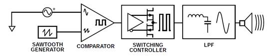
Basic Class D Amplifier Signal Flow
Audio amplifiers are divided into several categories: Class A, Class AB, Class B, and Class D. Class D amplifiers are highly efficient and provide high output power drive compared to other classes of amplifiers. Some commercial Class D amplifiers offer power capabilities ranging from 1500 W per channel to 6000 W per channel.
Class D amplifiers can be described simply as switching amplifiers or pulse width modulation (PWM) amplifiers. The figure below shows the signal flow of a basic Class D amplifier.
The operation of a typical Class D amplifier starts with a comparator. A standard analog audio signal with a frequency typically between 20 Hz and 20 kHz is compared to a high frequency triangular waveform to generate a PWM signal. The PWM signal then drives the output transistors, producing a series of pulses with potentially high voltages. Afterwards, a low-pass filter restores the sinusoidal audio signal. When not switching, the current through the output transistor is 0; the low on-resistance reduces I2R losses, thereby significantly reducing the overall power loss in the output stage. This enables high efficiency.
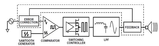
Even though Class D amplifiers have the advantages of high efficiency and high power operation, certain techniques can improve audio quality, such as the use of feedback and predistortion mechanisms. The figure below shows a basic Class D amplifier using a feedback mechanism. In the feedback mechanism, the output signal (usually from a filter) is sent to the error correction block at the input. Error correction modules can be fully analog, or use digital processing to intentionally predistort the audio signal to correct output artifacts and improve audio output quality. In addition to the inherent nonlinearity of the loudspeaker, the tendency of the loudspeaker impedance to change due to temperature and aging can also cause this imperfection.
The current monitoring circuit can obtain the data to be fed back for error correction. The challenge in choosing a device for this purpose is that the device must be robust enough to receive high-voltage pulses at the output of an audio amplifier. The AD8479 meets this requirement because it operates even in the presence of high input common-mode voltages. The ADA4805-1 is also added to the circuit as a low offset, low noise analog-to-digital converter (ADC) driver.
The AD8479 is a precision difference amplifier that can measure differential signals even in the presence of common-mode voltages up to ±600 V. The input common-mode voltage versus output voltage plot shown in Figure 3 demonstrates this capability. It has the following characteristics: low offset voltage, low offset voltage drift, low gain error drift, excellent common mode rejection ratio (CMRR) and wide frequency range. In this application note, the AD8479 is configured as a high-side current sense amplifier to monitor the current of a Class D audio amplifier. The AD8479 also has a bandwidth of 130 kHz to meet the bandwidth requirements of audio applications.
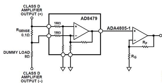
Current Monitoring Circuit Using AD8479 and ADA4805-1
The ADA4805-1 is a low input offset voltage and low input offset voltage drift rail-to-rail amplifier. The gain of the ADA4805-1 is set to 10 and the resulting output voltage is typically within the input voltage range below . Next, successive approximation (SAR) ADCs are often used to process audio signals. The class D amplifier used is a class D power amplifier with scalable output power from 25 W to 500 W. The amplifier is configured with a ±50 V supply voltage and provides a 1 kHz sinusoidal output. The AD8479 output is fed to the input of the ADA4805-1, which is used as an ADC driver with a gain of 10. Resistor tolerances should be low to avoid large offset drifts in the circuit.
For the Class D amplifier used in this circuit, the current through the sense resistor (RSENSE) is 4.74 A, resulting in a full-scale voltage of 475.71 mV peak. The common-mode voltage is 37.9 V peak.
Analysis of Main Error Sources in Current Monitoring
CMRR represents the ability of the device to reject common-mode interference signals at each input. Mathematically, it refers to the ratio of common mode gain change to differential gain. This parameter is often one of the large error contributors if high common-mode voltages are present, especially when measuring small differential signals. CMRR produces a corresponding output offset voltage error that is part of the total system error. The AD8479 has a specified CMRR of 96 dB. Another source of error is offset voltage. The smaller the full-scale signal, the larger the error contributed by the offset voltage.
The AD8479 has an input offset voltage of 1 mV, which when converted to ppm, contributes 2102 ppm of full scale (FS). The ADA4805-1 introduces an offset voltage of 125 μV, which is multiplied by a gain of 10, so the total error due to the offset voltage is 3352 ppm of full scale (FS). Also, the data sheet shows that the AD8479 has a gain error of 0.02% FS, so the AD8479 introduces an error of 200 ppm FS to the circuit.
Table 1 and Table 2 summarize the major error sources for the AD8479 and ADA4805-1, respectively. The AD8479 offset voltage contributes a large error, which is 2102 ppm FS at an input common-mode voltage of 37.9 V. The error contributed by the common mode voltage is 1262 ppm FS. Here, for a common-mode voltage of 37.9 V and a 0.1 sense resistor (see Figure 1), the offset voltage contributes the largest error, followed by the input common-mode voltage, but if the common-mode voltage is larger, it becomes a large source of error.For example, at 250 V a total of
At mode voltage, the common mode error contribution is 8329 ppm FS. This common mode voltage is common for high voltage Class D amplifiers. Also, the larger the sense resistor, the larger the voltage drop it causes, resulting in a higher full-scale voltage, which ultimately reduces all error contributions.
The figure below shows the response test results of the current sense circuit. It also includes the input voltage of the AD8479, the output voltage of the AD8479, and the amplified signal at the output of the ADA4805-1. About 4.74 A of current flows into the sense resistor and load. The signal at the inverting input is approximately ±38 V, and approximately ±500 mV appears at the AD8479 output, demonstrating the AD8479’s ability to measure differential signals in the presence of high common-mode voltages.
Measured current and voltage
Real-time monitoring requires not only high power devices, but also fast response to sudden changes in target current. The rate of change of the output signal must keep up with the rate of change of the input signal, which requires a correct interpretation of the electrical state of the loudspeaker, even a short circuit event, within a very short period of time.
The Links: SKM100GB124D DMG8601UFG-7 GETCOMPONENT
0 Comments for “Design of output current monitoring circuit for high-voltage class D amplifier for sound quality compensation and protection”