“In modern automotive electronics, there are generally multiple microcontrollers working together in coordination. DSP controller adopts Harvard structure and fast calculation speed, so DSP chip is widely used in automobile electronics to realize the control of automobile power system. ARM is a 32-bit microcontroller with abundant external expansion interfaces. Therefore, in automotive electronics, ARM is generally used to achieve the most large-capacity data storage and human-computer interaction or GPS global positioning system, so it is between DSP and ARM Need to exchange data.
“
In modern automotive electronics, there are generally multiple microcontrollers working together in coordination. DSP controller adopts Harvard structure and fast calculation speed, so DSP chip is widely used in automobile electronics to realize the control of automobile power system. ARM is a 32-bit microcontroller with abundant external expansion interfaces. Therefore, in automotive electronics, ARM is generally used to achieve the most large-capacity data storage and human-computer interaction or GPS global positioning system, so it is between DSP and ARM Need to exchange data.
CPLD (Complex Programmable Logic Device) is a complex user programmable logic device. Due to the use of hardware programmable technology, it is as convenient to design hardware circuits as software. DSP2407A is a microcontroller designed by T1 Company to meet a wide range of digital motor control applications. S3C4480 is a cost-effective microcontroller specially designed for handheld devices by Samsung. This design takes Xilinx’s XC95108 as an example, and realizes the parallel communication between DSP2407A and S3C4480 by opening up 2 independent SRAM areas (1 byte each) in the CPLD. Using this communication method, data transmission is accurate and high-speed, and can basically meet the requirements of real-time communication between DSP2407A and S3C4480 bus interface, thereby organically uniting vehicle power control and human-computer interaction.
1 Overall system structure design
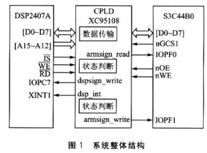
DSP2407A is responsible for collecting all the data of the car, and then sending the data to S3C44B0 through CPLD for data storage and human-computer interaction. Sometimes S3C4480 wants to receive the touch screen command, the command is also sent to the DSP2407A controller through CPLD, thus controlling the movement of the whole car. For DSP2407A, it is necessary to respond to the command sent by S3C44B0 in time; for S3C4480, it is necessary to receive the data sent by DSP2407A at any time. In this way, the real-time communication between the two parties must be very strong. Therefore, in system design, DSP2407A receives data in interrupt mode, and S3C44BO receives data in query mode.
In DSP2407A,[DO~D7]is the data line,[A15~A12]is the address line, IS is the I/O space strobe pin, when visiting the external memory or I/O space, it is the low level. WE is write enable, RD is read enable. IOPC7 is a general-purpose I/O pin for judging whether DSP2407A can write data to CPLD. When IOPC7 is low, it means that DSP2407A can write data to CPLD; if it is high, it means there is data in CPLD, and DSP2407A cannot write data to CPLD at this time. XINT1 is an external interrupt, used to notify DSP2407A to read the data in the CPLD.
In CPLD, use 1 piece of XC95l08 to realize. XC95108 has 108 macrocells in all, with enough space to realize two 8-bit SRAM areas; mainly used to realize data exchange between DSP2407A and S3C44B0, without setting the status bit of DSP2407A and S3C44B0 read/write control. In S3C44B0,'[D0~D7]is the data line, nGCSl is the chip selection signal, when the memory address is in the address area of the corresponding segment, the chip is activated. nWE is the write enable signal, and nOE is the read enable signal. IOPF0 is a general-purpose I/O port, used to monitor whether data can be read from the CPLD: when it is high, it means there is data in the CPLD, and data can be read; when it is low. Indicates that there is no data to read in the CPLD. IOPF1 is a general-purpose I/O port, used to monitor whether data can be written to the CPLD: when it is high, it means there is no data in the CPLD, and data can be written to the CPLD; when it is low, it means there is already in the CPLD Data, S3C44B0 cannot write data to CPLD. The system structure is shown in Figure 1.

2 CPLD design
Use Xilinx ISE8.1 as the design tool, and use the internationally universal VHDL language to write the source program.
2.1 8-bit data is transferred from DSP to ARM
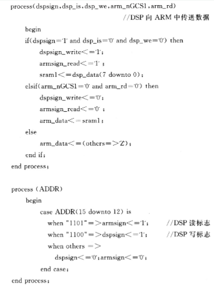
When[A15~A12]is 1100, DSP2407A starts to write data to CPLD, and sets dspsign_write and armsign_read to 1; indicating that there is data in CPLD, inform S3C4480 that data can be read and DSP2407A cannot write data to CPLD temporarily; At the same time, write data into the latch sraml.
When ARM sends out the read data signal, starts to read the data from sraml, and when dspsign_write and armsign_read are set to 0, it means that there is no data in CPLD, and DSP2407A can write data to CPLD again.

2. 2 8-bit data is transferred from 83CA480 to DSP2407A
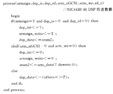
When S3C4480 writes data to the CPLD, it writes the data into the latch sram2, and at the same time sets dsp_int to 0 to notify the DSP2407A to generate an external interrupt, which can fetch data from the CPLD; set armsign_write to 0, indicating that there is data in the CPLD , S3C4480 can no longer write data to CPLD.
When[A15~12]is 1101, DSP2407A sends a read signal to CPLD, the data is transferred from latch sram2 to DSP2407A, and dsp_int is set to 1, armsign_write is 1, indicating that the data has been read by DSP2407A, S3C4480 You can continue to write data to the CPLD.

3 S3C4480 and DSP2407A communication software design
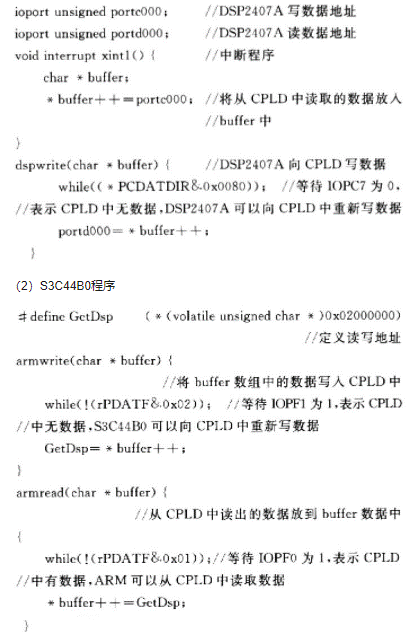
In this program, DSP2407A uses interrupt mode to receive data, and S3C4480 uses query port mode to receive data.
(1) DSP2407A program

The Links: NL128102BC28-01 BSM100GAR120DN2 LCD-SOURCE

0 Comments for “Design of Parallel Communication System Based on XC95108 Chip to Realize DSP and ARM”