“CMOS image sensor is a type of solid-state image sensor that has emerged in recent years. CMOS image sensor has low cost, low power consumption (1/1000~1/100 of CCD consumption), simple digital interface, random access, easy operation (single CMOS compatible battery supply), high speed (more than 1000 Frames per second), small size, and intelligent processing functions can be achieved through on-chip signal processing circuits, which have been widely used.
“
CMOS image sensor is a type of solid-state image sensor that has emerged in recent years. CMOS image sensor has low cost, low power consumption (1/1000~1/100 of CCD consumption), simple digital interface, random access, easy operation (single CMOS compatible battery supply), high speed (more than 1000 Frames per second), small size, and intelligent processing functions can be achieved through on-chip signal processing circuits, which have been widely used.
Some CMOS image sensors have a standard I2C bus interface, which can be easily applied to the system. Some dedicated CMOS image sensors without such bus interface circuits require an external drive circuit. Since most of the drive signals of CMOS sensors are digital signals, FPCA can be used to generate drive timing signals through Verilog HDL language programming. The Verilog HDL language is an IEEE standard hardware description language for logic design. It has a wide range of logic synthesis tool support and is concise and easy to understand. This article gives the logic drive circuit and simulation results designed using Verilog HDL language for STAR250, a CMOS image sensor.
1. CMOS image sensor STAR250
STAR250 is a CMOS image sensor specially designed for satellite celestial navigation star tracker (tracker). Due to the large amount of radiation in space, anti-radiation circuits are added to the chip to improve the reliability of space applications. The technical indicators of STAR250 are as follows:
(1) 0.5μm CMOS process;
(2) 512×512 resolution, pixel size 25μmx25μm;
(3) 4 photodiodes for each pixel to increase MTF (amplitude conversion function) and reduce PRNU (non-uniform light response);
(4) Anti-radiation design;
(5) On-chip double sampling circuit cancels FPN (fixed mode noise);
(6) Electronic shutter:
(7) Maximum 30 frames per second;
(8) You can take a sub-window;
(9) On-chip 10-bit ADC;
(10) Ceramic JLCC-84 pin package.
STAR250 is a line scan CMOS image sensor with active pixels. The outputs of all pixels are connected to the column bus, and each case has a column amplifier on the column bus. Using sub-sampling technology, the control column amplifier can subtract the residual charge from the last time the photosensitive cell was collected from the readout signal. The on-chip ADC is independent of the sensor and can be used or turned off by software while using an external ADC. STAR250 has a variety of data reading methods (window method, electronic shutter, etc.) for application convenience, and different reading methods have different timing requirements.
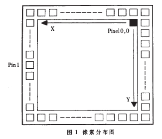
The image coordinate system of a traditional computer or printer defines the upper left corner as the origin (0, 0), and defines the upper right corner as the origin (0, 0) in STAR250, as shown in Figure 1. In this way, after the sensor outputs the digital signal, it can be easily converted into a computer format image, which is convenient for subsequent processing. The window scanning method is scanning from top to bottom and from left to right one pixel by one pixel.
2. STAR250 timing signal
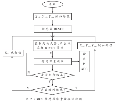
STAR250 completes image acquisition in two steps. The first step is to scan the RESET pixels line by line. After the pixel in the row is RESET, all photosensitive charges accumulated in the row since the last RESET or readout are drained. Start a new exposure cycle from the pixels in the RESET row. The second step is to read out the data of this exposure period. It is read in the form of voltage, and then converted to digital by ADC. Since the charge is read by draining, the pixel readout of the CMOS image sensor cannot be recovered, and the reading process is also equivalent to the RESET pixel, so the RESET speed of the CMOS sensor is the same as the read speed.
STAR250 calibrates the entire image address through three pointers: Yrd current scan line, Yrst current RESET line, Yrd current readout pixel. These three pointers have corresponding shift registers, and the size and position of the acquisition window can be adjusted by setting the initial values of these three registers. The flow chart of image acquisition is shown in Figure 2. The number of image frames per second is controlled by setting Yrd and Yrst, and the exposure period is also controlled by these two quantities. This amount of time can be expressed in terms of space distance (line spacing), which defines DelayLines=Yrst-Yrd+. Since the RESET and read time of each line are fixed, if DelayLines is fixed, the frame rate is also fixed. The effective integration time (exposure time) that converts DelayLines into pixels is the time taken to read a row of pixels by multiplying Delay-Lines. The time it takes to read a row of pixels consists of four parts: (1) the number of effective pixels in the row (defined by the length of the row); (2) the time it takes to read a pixel; (3) the accumulated charge of the pixel is converted to a number The amount of time; (4) The time it takes to select a new line. For example, when the main clock frequency is 12MHz, the output frequency of the pixel is divided by 2 of the main clock 6MHz, so the time required for a row of pixels is 512×1/6MHz=85.3μs. Coupled with the time required for line feed, the reading time for a line of pixels is about 90 μs. Therefore, you can set DelayLines according to this time to control the exposure time.
3. Verilog HDL drive timing design
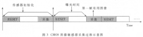
Through the above analysis, it can be seen that the CMOS image sensor can be divided into the RESET process and the acquisition process. The two processes are independent in time, as shown in Figure 3. But the circuit that processes these two parts in the FPGA physically exists at the same time, so the corresponding signal must be set to be valid or invalid by setting the flag.
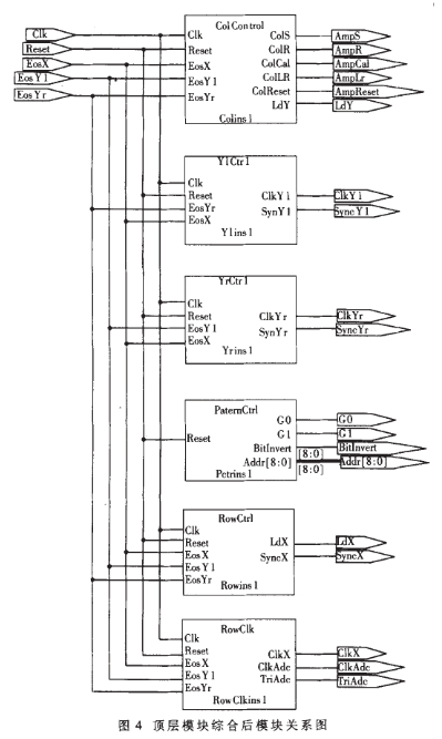
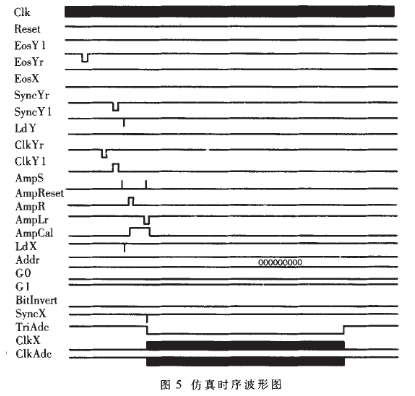
STAR250 requires a total of 28 digital drive signals, of which the SELECT signal is directly connected to the Vcc of the PCB board when in normal use. Therefore, there are 27 driving signals that need to be controlled by FPGA. According to the acquisition process, the signal can be divided into column amplifier signals, including CAL, Reset, Lr, S, R, and LdY. These 6 signals are used in the initialization part of each row, so they can be programmed into a module (ColControl); the mode signal (PaternCtrl) module is used to set the working mode and initial address of the CMOS sensor, including G0, G1, and G1. Bitlnvert and Addr[8:0]have a total of 12 signals. Among them, G0 and G1 are used to design the output magnification, BitInvert is used to invert the output, and Addr[8:0]sets the start address of the collection; the row readout signal control module (YlCtrl) generates the synchronization of the row readout address Signal SyncYl and clock drive signal ClkYl; Row RESET signal control module (YrCtrl) generates row RE-SET address synchronization signal SyncYr and clock drive signal ClkYr; Pixel control module (RowCtrl) generates row pixel initial address loading signal LdX and synchronization signal SyncX; the row clock signal module (RowClk) generates the clock drive CLKX of the pixel in the column, the ADC drive clock signal CLkAdc and the output tri-state control signal TriAdc. The input signal of the system is the main clock CLK, EosX pixel end signal in line, EosYl frame end line signal, EosYr frame RESET line end signal, and chip RESET signal. The modular Verilog program after this division is easier to write. The netlist generated through the synthesis of the top-level module is shown in Figure 4. The wiring simulation timing diagram is shown in Figure 5, where the clock signals are too dense and become black bands, and the output clocks CIkX and ClkAdc are also black bands. In terms of timing, ClkX and ClkAdc have an inverse relationship, and the output is valid when TriAdc remains low. The designed simulation waveform of the driving signal is very consistent with the theoretical waveform. This completes the timing drive circuit design of STAR250.
The use of Verilog language to design sequential logic has very high efficiency. Combining the characteristics of CMOS sensors can easily develop drive sequential circuits. But it is necessary to accurately analyze the signal of the CMOS image sensor, correctly separate those independent signals and shared signals, use sequential logic to design the drive signal, and use combinational logic to realize the time separation of different acquisition processes. The wiring delay must be considered, and the pipeline technology can be used to predict the delay and ensure the correctness of the signal. Although the storage circuit of the pixel ADC output is not given in the article, in fact, the TriAdc signal is directly used as the chip selection of SRAM, the low level of ClaAdc is used as the write signal, and the address of SRAM is increased on the rising edge of ClkAdc and written on the falling edge. In this way, the storage of image data can be completed. The above Verilog program is realized by wiring on FLEXl0kl0. Observed by an oscilloscope, the logic is correct, and the CMOS sensor works normally.
The Links: CM100TJ-24F LM64K112
0 Comments for “Logic drive circuit and simulation design based on STAR250 CMOS image sensor”