“In a successful power supply design, the power supply layout is an important part of it. However, everyone has their own opinions and reasons for how to do this. The fact is that many different solutions have the same goal; if the design is not really messed up, most power supplies will work properly.
“
In a successful power supply design, the power supply layout is an important part of it. However, everyone has their own opinions and reasons for how to do this. The fact is that many different solutions have the same goal; if the design is not really messed up, most power supplies will work properly.
Of course, there are also some general rules, such as:
Do not run sensitive signals in fast switching signals. In other words, do not run feedback tracking under the switch node.
Ensure that the power load tracking and ground plane are large enough to support the current current.
Try to maintain at least one continuous ground plane.
Use enough vias (usually starting with 1A per via) to connect the ground plane.
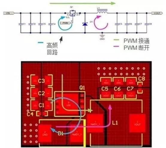
In addition to these basic layout rules, I usually first identify the switching loops and then determine which loops have high-frequency switching currents. Figure 1 shows an example of a simplified power stage for a step-down power supply (schematic and layout).

Figure 1: Schematic diagram and layout of the step-down power supply
There are two states in the step-down power supply (assuming continuous conduction mode): when the control switch (Q1) is on and when the control switch is off. When the control switch is turned on, current flows from the input to the inductor. When the control switch is turned off, current continues to flow in the inductor and through the diode (D1). Continuous current output.
But there is input pulse current, which is the part you need to pay attention to in the layout. In Figure 1, this loop is labeled “High Frequency Loop” and shown in blue. The primary goal of your layout is to connect Q1, D1 and the input capacitor to a short, low-inductance loop. The smaller the loop, the lower the noise generated by the switch. If you ignore this, the power supply will not work effectively.
The procedures for identifying switch circuits are applicable to all power supply topologies. The various steps of the procedure are:
• Determine the current path in the on state.
• Determine the current path in the disconnected state.
• Find the location of continuous current.
• Find the location of the intermittent current.
• Minimize intermittent current loops.
The key loops for a given power stage configuration are listed in this list:
• Step-down-input capacitor circuit.
• Boost-output capacitor circuit.
• Inverting buck-boost-input and output capacitor loops.
• Flyback—input and output capacitor loops.
• Fly-Buck?-Input capacitor circuit.
• SEPIC-output capacitor circuit.
• Zeta-input capacitor circuit.
• Forward, half bridge, full bridge-input capacitance loop.
Power layout is like an art form, everyone has their own way, and it will work in many cases. One thing to ensure is that when you determine the location of the power stage parts, first determine the high-frequency switching circuit; this way you can save yourself time and worry.
The Links: LTA084C271F ADS62P15IRGCT

0 Comments for “Power supply layout, an important part of the success of power supply design”