Semiconductors enter the 3nm era
In 2020, Samsung announced that it has completed the development of 3nm technology. With the successful tapeout of 3nm, it also means that the time for final mass production will be getting closer and closer.
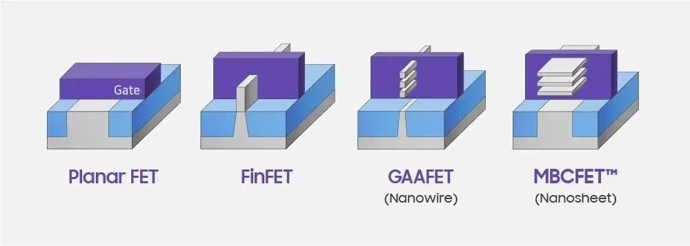
FinFET architecture has been the mainstream of reports over the past few years, not only by Intel, since Intel first adopted it at the 22nm node. semiconductor giants including TSMC have adopted this architecture.
As the semiconductor process moves from 5nm to more advanced processes, the FinFET structure has been difficult to meet the current driving and electrostatic control capabilities required by transistors. It is generally believed that the GAA architecture will become the mainstream of advanced processes in the future.
Samsung announces successful 3nm tapeout
The progress of Samsung’s 3nm process tapeout is to cooperate with Synopsys to accelerate the provision of a highly optimized reference method for the production process of the GAA architecture.
Because Samsung’s 3nm process based on GAA technology is different from TSMC’s 3nm process of FinFET architecture, Samsung needs new design and certification tools, so it uses Synopsys’ Fusion Design Platform.
This process is expected to make Samsung’s 3nm GAA structure process technology available for high-performance computing (HPC), 5G, mobile and high-end artificial intelligence (AI) application chip production.
The GAA transistor structure represents a critical inflection point for process technology advancement and is critical to sustaining the strategies needed for the next wave of hyperscale innovation.
Synopsys and Samsung’s strategic partnership supports the delivery of best-in-class technologies and solutions, ensuring the continuation of trends and opportunities for the semiconductor industry.

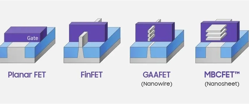
Samsung believes that the use of nanowire channel design is not only complicated, but also the cost may outweigh the benefits. Therefore, Samsung designed a new form of GAA-MBCFET (Multi-Bridge-Channel FET, multi-bridge-channel field effect transistor), using multi-layer stacked nanosheets to replace the nanowires in GAAFET.
This nanosheet design has been extensively studied by research institute IMEC as a follow-up to the FinFET architecture, and developed by IBM in collaboration with Samsung and GlobalFoundries.
According to Samsung, compared to the 5nm manufacturing process, the 3nm GAA technology improves logic area efficiency by more than 35%, reduces power consumption by 50%, and improves performance by about 30%.
Samsung announced the PDK physical design kit standard for the 3nmGAA process as early as 2019. This time, the 3nm chip tape-out was completed in cooperation with Synopsys. The two parties jointly verified the design and production process of the process, which is a milestone for the 3nmGAA process.
Samsung’s action caught TSMC off guard
TSMC will not be able to enter the 3nm mass production stage until the second half of next year, and the tape-out time is expected to wait until next year. However, Samsung also took the lead in realizing the 3nm tape-out work.
According to the news from Samsung, the 3nm process chip adopts the GAA architecture, and its performance is better than that of TSMC’s FinFET architecture.
This shows that on the same process, Samsung’s 3nm chip performance is even better than TSMC. After the tape-out is completed, Samsung is also approaching the mass production of 3nm chips.
It is estimated that TSMC also did not expect this. Originally, TSMC took the lead every time. As a result, Samsung suddenly emerged, bringing news of the success of 3nm tape-out.
Samsung helped Qualcomm manufacture the Snapdragon 888, a chip widely used in the high-end mobile phone market. The better the chips are sold, the greater the profit for Samsung’s foundry.
If the follow-up 3nm customer is still Qualcomm, Qualcomm’s position in the mobile phone market will definitely bring Samsung a huge market share. At that time, TSMC will have a certain pressure.
TSMC has said that its 3nm chip process has achieved technological breakthroughs and is expected to achieve mass production by the end of next year, and will give priority to customers such as Apple.
TSMC has more than half of the world’s chip production capacity, and it has promised to build 6 new chip factories in the United States in one breath, showing its confidence and strength.
Now it seems that TSMC’s statement seems outdated and premature. Samsung’s news about 3nm chips may ruin TSMC’s plans.
There has been a lot of bad news from TSMC recently. First, its sub-factories were unable to OEM due to certain problems, which caused TSMC to lose a lot of orders. Second, the United States suddenly pulled TSMC into the blacklist, which caught TSMC by surprise.
Being blacklisted by the United States is not the most deadly, after all, TSMC has withdrawn its factory in the United States; but if Samsung’s 3nm tape-out is successful, it will enter the mass production stage, which means that Samsung may overtake here and become the first energy A foundry that produces 3nm chips.
Samsung increases investment and competes with TSMC for advanced manufacturing process
In the field of global chip foundry processing, most of the global chip foundry orders are divided by the two of them, and the rest of the chip foundries can only compete for the remaining orders from the two of them. These two are also known as the global semiconductor foundry double male.
For a long time, TSMC and Samsung have competed with each other in terms of advanced chip process technology, and they are in a situation where you are catching up. Generally speaking, almost TSMC has the upper hand, followed by Samsung, and the gap is not very obvious.
In late May of this year, TSMC revealed that its 3nm chip process technology research and development progress is rapid, and it is expected that trial production will be possible in the second half of this year, and by the end of next year, large-scale mass production can be achieved.
In the performance test, the GAA architecture transistor has better performance, which is better than the FINFET architecture adopted by TSMC’s 3nm process. Even if both parties have mastered the 3nm process chip manufacturing, Samsung’s 3nm chips are better than TSMC’s 3nm chips. It is understood that Samsung’s 3nm chips The performance of the chip is 30% higher than that of the 5nm chip, and the power consumption is reduced by 50%.
Samsung’s overtake of TSMC this time is not accidental, but inevitable. Samsung has disclosed before that South Korea will invest 171 trillion won in the non-memory chip field, which is equivalent to RMB 979 billion at the exchange rate. Achieve the goal of becoming a chip power by 2030.
Can Samsung’s 10-Year Goals Be Achieved?
Samsung is already accelerating its pace. Although TSMC has a leading edge in production capacity and market share, Samsung has not given up catching up. The goal is to surpass TSMC to become the world’s largest chip maker within the next decade.
In this regard, Samsung also increased its investment before 2030 to 151.4 billion US dollars, and increased investment in the non-memory chip field. Compete directly with TSMC and surpass TSMC in one fell swoop.
Judging from the current development trend of Samsung, it has already threatened the status of TSMC in a certain technical field. If Samsung can greatly increase its production capacity and stabilize the yield, it may shorten the distance from TSMC’s market share.
If Samsung can achieve mass production of 3nm chips by the end of the year, it will not be good news for TSMC. We can only rely on TSMC’s 3nm chips to be mass-produced faster than Samsung, which can also grab market share, otherwise it may be the world’s first The location of the big chip foundry is going to Samsung.
end:
Samsung’s decision to use this technology this time is making a big gamble. If the gamble is lost, then Samsung is likely to bring TSMC to become the world’s largest chip foundry.
But if the bet is lost, then Samsung’s goal of surpassing TSMC may be further away.
Now that Samsung has achieved the tape-out of this 3-nanometer chip, to a large extent, it means that Samsung has completed its dream of overtaking in a corner. Of course, this is only limited to 3-nanometer chips.
As for what kind of actions TSMC will make next, we will wait and see.
Part of the data reference: Xinzhixun: “Leading TSMC, Samsung’s 3nm GAA process successfully taped out! What is GAA?”, Artificial Intelligence Scientist: “Heavy! Samsung announces 3nm successful tapeout!”
The Links: NL2432HC17-09B 2MBI150N-060


0 Comments for “Samsung announces successful 3nm tapeout, competing with TSMC for advanced process”