“Wirelessly networked devices convert electrical signals into electromagnetic waves and vice versa through radio frequency radios, antennas and associated circuits. The designer has two options to implement the circuit: a) use an RF chipset and design the associated RF section; b) use a module that already has the RF chipset and associated RF section installed. In this article, we will compare the two approaches and help designers make an informed decision.
“
Vishal GOYAL
Technical Marketing Manager
South Asia and India
STMicroelectronics
introduction
Stastita[1]It is predicted that by 2025, the number of IoT devices will exceed 75 billion, far exceeding the United Nations forecast of the global population of 8.1 billion in 2025[2]. The Internet of Things may be one of the biggest enablers for tech companies. The most important feature of IoT devices is networking.
Wirelessly networked devices convert electrical signals into electromagnetic waves and vice versa through radio frequency radios, antennas and associated circuits. The designer has two options to implement the circuit: a) use an RF chipset and design the associated RF section; b) use a module that already has the RF chipset and associated RF section installed. In this article, we will compare the two approaches and help designers make an informed decision.
RF section using chipsets and modules
The RF part realized by the chipset is composed of RF IC, antenna, balun and filter, matching network, crystal oscillator, and other passive components.Below is a reference implementation schematic using ST’s BlueNRG BLE SoC
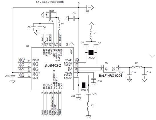
Figure 1: BlueNRG-2 reference schematic
The implementation using the module approach is much simpler. The same circuit as in Figure 1 can also be implemented using off-the-shelf modules. Below is the pinout and internal block diagram of ST’s BlueNRG-M2SA module. The module is implemented using the BlueNRG-2 SoC and associated circuits.
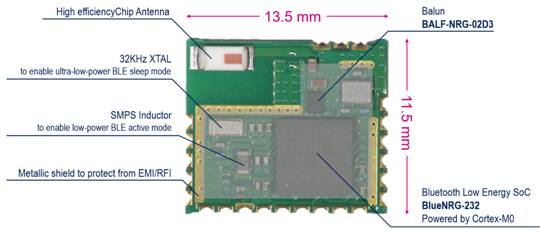
Figure 2: BlueNRG-M2SA pin assignment and internal block diagram
Comparing the Chipset Approach to the Module Approach
There are three main aspects to consider when choosing an appropriate method: a) time-to-market, b) certification, and c) cost. We will review each aspect so that it can be understood logically.
time to market
The steps to design the RF section using the chipset are as follows:
i) Design schematic and layout
ii) Ask the PCB manufacturer to make the board
iii) Welding plate
iv) Fine tune the values of passive components to optimize performance
v) Order all components of the module and then produce the module
vi) RF Testing and Certification
The RF part of the chipset based design takes almost 3-6 months. It also requires multiple resources such as RF designers, supply chain and multiple service partners such as PCB manufacturers and EMS companies. This method is suitable for high volume production, but not for prototyping and small batch production.
Modules are designed for quick time-to-market. Adding connectivity using modules does not require any RF expertise. The wireless connection is relatively simple, like a modular plug-and-play component, because the designer gets an off-the-shelf RF part, and the modular implementation is very fast. As a result, designers can bring their products to market very quickly. This is especially important for prototyping and low-volume production.
Certification
Almost any Electronic device is subject to universal emissions testing. In addition, devices with radio frequency parts are also considered to be intentional emitters. Therefore, they require additional certification to ensure that they do not radiate more power than allowed, or interfere with other devices or frequency bands. In this regard, there is no universal certification, and each country or region has its own standards. Often these criteria are similar, but they still need to go through the application and associated process.
Additionally, most RF technologies, such as BLE, Wi-Fi or GPRS, must conform to standards set by specific organizations. So, they also have to pass these certifications. For example, the certification process for ST’s BlueNRG SoC and BlueNRG-M2SA modules.
Bluetooth low energy devices need to be certified by the Bluetooth SIG, the body that governs the use of the Bluetooth logo. They also need to obtain RF certification from different countries and regions. The certifications identified in some countries and regions are FCC (United States), RED (Europe), WPC (India), IC (Canada), SRCC (China), and Type (Japan).
Since the module has been tested and certified as a radiant device, a design implemented with a module does not need to be certified as a radiant device and can be considered a derivative of the module used. Below is a cost comparison between the chipset approach and the modular approach.
The certification process is time-consuming, cumbersome and costly. If the volume is large enough, the cost can be spread through economies of scale, but for small batches, the spread of the cost is too high.
cost
Some elements of cost have been discussed in this article.Generally speaking, the cost includes
circuit design cost
Designer costs, supply chain costs and production costs
Certification cost
opportunity cost
In general, these costs are reasonable if the annual output exceeds 100-150K pieces, or if the shape of the product does not allow the use of specialized modules.
Modules from STMicroelectronics
STMicroelectronics is the world’s leading semiconductor company producing a wide range of low-power RF devices and modules.The RF chipsets and related modules offered by STMicroelectronics are shown in the table below
|
Technology |
IC |
module |
instruction |
|
BLE |
BlueNRG-MS Network Processor |
BlueNRG-M0A |
Full function/low power consumption |
|
BlueNRG-M0L |
low cost |
||
|
BlueNRG-2 application processor |
BlueNRG-M2SA |
Full function/low power consumption |
|
|
BlueNRG-M2SP |
low cost |
||
|
RF SubGhz 433MHz, 868Mhz, 915Mhz |
SPIRIT1 small wireless |
SPSGRF-868/915 |
Built-in antenna |
|
SPSRFC-433/868/915 |
UFL connector for external antenna |
A very important aspect to consider is that all the chipsets and modules mentioned above are included in the 10-year long-term availability plan. This means that if a company uses these components in its designs, ST will continue to supply these components for 10 years from the product launch date, or provide fully compatible replacements.
in conclusion
If the shape of the end device does not fit the module or the volume is very large, a chipset approach should be used to achieve reasonable design cost, production cost and certification cost. If a company wants to focus on its core competencies and avoid the hassles of RF design, a modular approach should be the first choice. The modular approach is also preferred for prototyping and small batch production. As described in this article, STMicroelectronics is a leader in low-power RF technology, offering a wide range of chipsets and modules for a variety of application scenarios.
The Links: PM50CS1D060 EL640.400-C2-FRA
0 Comments for “ST Connected Chipsets or Modules for IoT Systems Can Solve RF Design Challenges”