“For self-driving cars to succeed, users must believe that car sensors and software are safe and accurate enough to guide them to their destinations. The key to achieving trust lies in the fusion of inputs from different types of sensors to improve accuracy, redundancy and safety. Advanced driver assistance systems (ADAS) use this technology. One of the main sensors is LiDAR, and designers need to ensure that the LiDAR system has the highest reliability, resolution, accuracy, and response time.
“
For self-driving cars to succeed, users must believe that car sensors and software are safe and accurate enough to guide them to their destinations. The key to achieving trust lies in the fusion of inputs from different types of sensors to improve accuracy, redundancy and safety. Advanced driver assistance systems (ADAS) use this technology. One of the main sensors is LiDAR, and designers need to ensure that the LiDAR system has the highest reliability, resolution, accuracy, and response time.
The performance of Lidar relies heavily on the front-end transimpedance amplifier (TIA), which can quickly restore the avalanche photodiode (APD) signal and provide digital feedback. By comparing the time stamp of the feedback signal with the time stamp of the transmission signal, the time of flight (ToF) can be calculated for ranging.
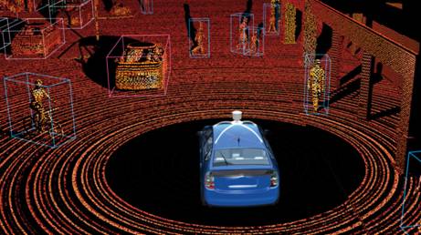
This article will briefly discuss the issues related to the performance of the feedback circuit for the use of lidar for accurate target detection. Then introduce an analog device TIA. It will show how to use its high speed, bandwidth, and low input impedance to quickly recover from reflected light, resulting in a nanosecond (ns) photodiode rise time. In order to obtain the best overall performance, this article will also show how to reject APD dark current and ambient light through AC coupling to achieve accurate ToF estimation.
Key elements of ADAS
The core of ADAS is a complex sensing system that analyzes external objects. Identifying and locating these objects allows the vehicle to notify the driver to take appropriate actions to avoid accidents. The sensor technology behind ADAS includes image cameras, inertial measurement units (IMU), radar, and of course lidar. Among them, Lidar is a key optical technology, which can be used for sensing and measuring distances of autonomous vehicles in inclement weather and lateral distance. It is an integral part of the ADAS system.
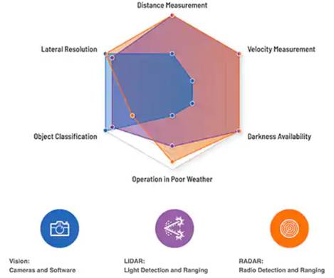
Vision equipment (camera), radar and lidar systems complement each other to inform ADAS so that it can take appropriate actions.
The ADAS system uses cameras to quickly and accurately detect and identify external objects such as vehicles, pedestrians, obstacles, traffic signs and lane lines. The analysis triggers the appropriate response to maximize safety. Response measures include lane departure warning, automatic emergency braking, blind spot warning, driver awakeness and warning monitoring. The advantages of this camera are target classification and lateral resolution.
The self-contained IMU system measures angular motion and linear motion. The system usually uses a gyroscope, magnetometer, and accelerometer. The IMU frame can reliably output the integral angular velocity and acceleration. A gimbal (also known as a gimbal) is a pivotal support that allows objects to rotate around a single axis. This is a set of three frames, one mounted on the other, with orthogonal axes, allowing objects mounted on the innermost frame to keep rotating independently of its support. IMU improves the accuracy of GNSS from meters to centimeters to achieve accurate lane positioning.
Automotive radar technology can measure many different variables, including distance and speed, while also providing “visibility” in the dark. Generally, signal rates of 24 and 77 GHz are used for high resolution. The radar sensor captures the signals reflected by different objects in its field of view. The vehicle then analyzes the sensor output in the context of all other sensor inputs to determine whether steering and braking need to be adjusted, for example, to prevent collisions.
To complete ADAS images, lidar uses optics with a spectral response range of 200 to 1150 nanometers. The system receives the reflected signal through laser emission and measures ToF. Through the compilation of multiple signals, an accurate multi-dimensional depth map of the surrounding environment of the vehicle can be generated. Lidar applications include collision avoidance, emergency braking, adaptive cruise control, dynamic suspension control, and parking assist. Under severe weather conditions, lidar systems surpass radars in terms of lateral resolution and capabilities.
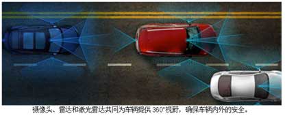
ADAS and autonomous vehicles need to place multiple such sensors around the vehicle for 360˚ detection and analysis.
Optical Technology of Lidar
The design of lidar has evolved from a “coffee can” sensor (worth about $75,000) rotating on the roof of the car to a more modern approach, with each sensor costing about $1,000. The cost reduction benefits from the advancement of laser and related Electronic technology, as well as the development of semiconductor lasers and the scaling and size reduction of transistors. The biggest contribution is MEMS. For lidar, the greatest value of MEMS lies in the fact that in order to achieve scanning by mechanical lidar, the laser transmitter must be rotated. The MEMS micro-electromechanical system can directly integrate a very compact micro galvanometer on the silicon-based chip, and the rotating micro galvanometer reflects the light of the laser to realize scanning. In this way, the lidar itself does not need to be rotated substantially, which can effectively reduce the probability of problems in the driving environment of the entire system.
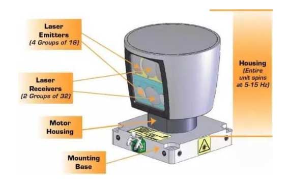
Compared with mechanical lidar, the biggest structural feature of solid-state lidar is that it has no rotating parts and is relatively small. Now, multiple lidar sensors can be installed on the front, back and sides of the vehicle to obtain a cost-effective 360˚ visibility.
Lidar is composed of three parts: transmitting system, receiving system, and information processing. The working principle of lidar is to use visible and near-infrared light waves (mostly infrared light near the 950nm band) to emit, reflect and receive to detect objects. According to the structure, lidar is divided into mechanical lidar, solid-state lidar and hybrid solid-state lidar.
Mechanical Lidar: The launching system and the receiving system rotate in a macro sense, that is, by continuously rotating the launching head, the faster and more accurate launching laser is changed from “line” to “plane”, and in the vertical direction Multiple lasers are arranged on the top to form multiple surfaces to achieve the purpose of dynamic scanning and dynamic receiving of information.
Solid-state lidar: One host supports multiple probes, the probe is small in size, has no mechanical rotating parts, adopts MEMS technology route, has a long service life in harsh environments, and meets demanding vehicle-level requirements (at least 50,000 hours) ), impact resistance, anti-bumps, and 3D Flash technology has a shorter detection distance, and the effective detection distance is roughly 20-30m.
Hybrid solid-state lidar: refers to the use of semiconductor “micro-motion” devices (such as MEMS scanning mirrors) to replace the macro-mechanical scanner, and realize the laser scanning method of the radar transmitting end on the micro-scale. The MEMS scanning mirror is a silicon-based semiconductor component, which is a solid-state electronic component; but the MEMS scanning mirror is not “secure”, it integrates a “movable” micro-mirror; it can be seen that MEMS scanning mirrors are both “solid-state” And the two attributes of “movement”, so it is called “mixed solid state”.
Lidar work breakdown
A typical lidar design can be divided into three main parts: data acquisition (DAQ), analog front end (AFE) and laser source.
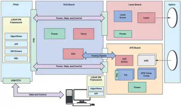
DAQ contains a high-speed, low-noise precision analog-to-digital converter (ADC) and corresponding power and clock to collect ToF data from the laser and AFE. AFE includes APD avalanche diode light sensor and TIA to capture the reflected signal. The entire signal chain conditionally processes the APD output signal, which is fed back to the ADC in the DAQ part. AFE also includes delay timing in its output to DAQ.
Lidar AFE
As shown in the figure, the lidar receiver signal chain starts with high voltage reverse bias (-120 to -300 volts), low input capacitance APD and TIA, such as ADI’s LTC6561HUF#PBF. The key point is to design a lower APD input and pc board parasitic capacitance to supplement TIA’s high-speed 220 MHz gain bandwidth product (GBWP). The TIA input part requires additional attention to achieve the required signal integrity and channel isolation level, so that the current signal generated by the APD has no additional noise, and maximizes the system’s signal-to-noise ratio and target detection rate.

In order to enhance signal integrity, TIA has a low-pass amplifier filter, ADI’s LT6016, which can suppress high-speed signal ringing. TIA converts the APD output current (IAPD) into the output voltage VTIA. The voltage VTIA is transmitted to the differential buffer amplifier (ADA4950-1YCPZ-R7 from ADI) to drive the input of the ADC.
Use ToF to calculate the distance, use the increment of ADC sampling rate to determine the resolution of the received light pulse, formula 1: ![]()
LS = Speed of light (3 x 10⁸ m/s)
fS = ADC sample rate
N = the number of ADC samples in the time interval between the generation of the light pulse and the reception of its reflection
For example, if the sampling rate of the ADC is 1 GHz, each sample corresponds to a distance of 15 cm.
The sampling uncertainty must be close to zero, because even a small amount of uncertainty samples can cause considerable measurement errors. Therefore, the lidar system uses parallel TIA and ADC to drive zero sampling uncertainty. The increase of the channel improves the power consumption and the size of the pc board. These key design constraints also require a high-speed serial output ADC with a JESD204B interface to solve the parallel ADC problem.
Lidar sensor
As mentioned earlier, the key sensor element of the lidar system is APD. The reverse voltage bias range of these photodiodes with internal gain is between tens of volts to hundreds of volts. The signal-to-noise ratio (SNR) of APD is higher than that of PIN photodiodes. In addition, the fast response, low dark current and high sensitivity of APDs make them stand out. The APD spectral response range is 200 ~ 1150 nm, which is in line with the typical spectral range of lidar.
Take MTAPD-07-010 from Marktech Optoelectronics as an example. Its spectral response ranges from 400 to 1100 nm, with a peak at 905 nm. The effective area of the device is 0.04 millimeter square (mm2). It dissipates 1 milliwatt (mW), has a forward current of 1 milliampere (mA), and a breakdown voltage (Vbr) of 0.95 times the working voltage of 200 volts (maximum). Its rise time is 0.6 ns.
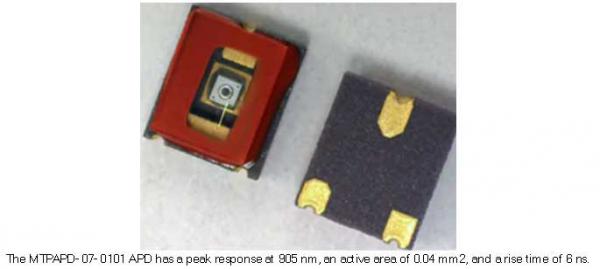
The reverse voltage of a typical semiconductor APD is between tens of volts or even hundreds of volts, sometimes lower than the breakdown voltage (MTAPD-07-010 at 0.95 Vbr). In this structure, the absorbed photons excite electrons and holes in the strong internal electric field, generating secondary carriers. In the range of a few microns, the avalanche process effectively amplifies the photocurrent.
Due to its operating characteristics, APD requires less electronic signal amplification, so that it is less susceptible to electronic noise, making it suitable for very sensitive detectors. The multiplication factor or gain factor of the silicon APD depends on the device and the applied reverse voltage. The gain of MTAPD-07-010 is 100.
TIA’s solution
In operation, the lidar emits a digital pulsed light signal, and its reflection will be captured by the MTAPD-07-010 APD. This requires TIA to have fast saturation overload recovery time and fast output multiplexing. The LTC6561 low-noise, four-channel TIA with a bandwidth of 220 MHz meets these requirements.
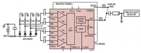
The reflected laser signal is captured by the APD array and four low-noise 200 MHz TIAs. TIA quickly transmits the captured signal to the ToF detector (upper right corner). The 1 nanofarad (nF) capacitors on the 4 TIA inputs effectively filter the APD dark current and ambient light conditions, maintaining the dynamic range of the TIA. However, the value of the capacitor will affect the switching time, so designers need to take this into consideration when designing.
Under strong optical illumination, APD can conduct large currents, usually more than 1 ampere. LTC6561 can quickly recover from large overload currents of this magnitude. Fast overload recovery is the key to lidar applications. Fast recovery from 1 mA overload takes 10 nanoseconds.
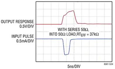
When the input current level exceeds the linear range, the output pulse width becomes wider. But the recovery time remains at 10 (ns). The LTC6561 recovers from a 1 mA saturation event and reverses phase in less than 12 mA seconds, thereby minimizing data loss.
in conclusion
The road to success for autonomous vehicles begins with the integration and fusion of cameras, IMUs, radars, and lidars. Especially lidar, when the related problems of using this optical technology to achieve accurate target detection are understood and fully resolved, it has hope.
The Links: PM200DSA060 LMG5271XUFC-D

0 Comments for “The key factor that determines the performance of Lidar: front-end transimpedance amplifier”