“In the field of civil wireless communication applications, due to the continuous development and wide application of short-range wireless communication systems, the resources of the ISM frequency band exempted from application are becoming more and more tense, the frequency overlap between systems is also increasing, and system interference is also increasing. It is more and more serious, so it has very direct practical significance to design a civil anti-jamming communication system with frequency hopping function. Using this technology can not only improve the anti-interference ability of the system, but also greatly reduce the complexity of system maintenance.
“
Authors: Zhai Leyu; Peng Li; Huang Weiping
introduction
In the field of civil wireless communication applications, due to the continuous development and wide application of short-range wireless communication systems, the resources of the ISM frequency band exempted from application are becoming more and more tense, the frequency overlap between systems is also increasing, and system interference is also increasing. It is more and more serious, so it has very direct practical significance to design a civil anti-jamming communication system with frequency hopping function. Using this technology can not only improve the anti-interference ability of the system, but also greatly reduce the complexity of system maintenance. The frequency hopping communication system is mainly composed of signal modem, frequency hopping pattern generator, frequency synthesizer and frequency hopping synchronizer. This paper mainly introduces the civil anti-jamming slow frequency hopping communication system.
1 How it works
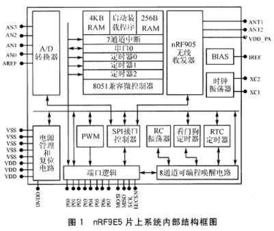
The internal structure of nRF9E5 is shown in Figure 1. The main components of the system-on-chip integration are: 8051-compatible microprocessor, 4 KB RAM and related special function registers (SFR), 4-input channel 10-bit 80 ksps A/D converter, 433/868/915 MHz nRF905 Wireless transceivers, power management and reset circuits, PWM controllers, SPI interface controllers, low-power mode RC oscillators, watchdog timers, port logic and RTC timers, and more. The microprocessor is connected to the A/D converter and the wireless transceiver through the SPI interface. The microprocessor program is solidified in the external EEP-ROM memory. When the system is powered on, the boot program loads the firmware into the chip through the SPI interface. In the internal 4 KB RAM area, the system is controlled by the on-chip RAM program after the program is loaded. The RF signal output power of the chip is programmable, the maximum output is 10 dBm, the channel conversion time is less than 650 μs, it has the carrier monitor function, and supports the LBT (Listen Before Trans-mit) protocol.
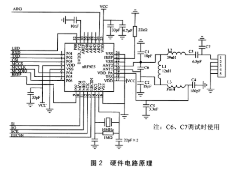
The integrated wireless transceiver in nRF9E5 can work in the frequency range of 433/868/915 MHz. The specific working frequency band and frequency point are determined by the resistance-capacitance parameters of the peripheral circuit and the relevant register data. In the circuit shown in Figure 2, if the system is required to work in the 433 MHz frequency band, the related devices should take the value in the second column of Table 1; if the system requires the system to work in the 868/915 MHz frequency band, the related devices should take the value in the third column. . The operating frequency band of the system is not only configured by hardware, but also set in the corresponding RF configuration register. Among them, HFREQ_PLL sets the working frequency band, CH_NO sets the working frequency point, HFREQ_PLL is a control bit, and CH_N0 is 9-bit data. The specific wireless carrier frequency is calculated by the following formula:
fOP=[422.4+(CH_NO/10)]×(1+HFREQ_PLL)
The unit of fOP in the formula is MHz. If HFREQ_PLL=O, the system works in the 433 MHz frequency band, the frequency point interval is 100 kHz, and the frequency band range is 422.4 ~ 473.5 MHz; For 844.8 ~ 947 MHz. It can be seen that if the system program sets CH_NO according to the pseudo random number generated by the frequency hopping pattern, the nRF9E5 can realize anti-interference frequency hopping communication of 512 frequency points in 2 frequency bands respectively.
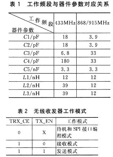
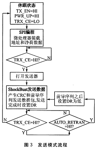
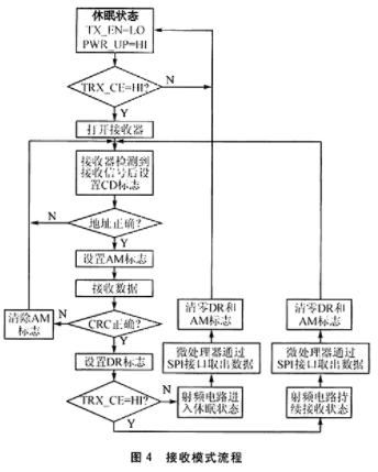
The integrated wireless transceiver in nRF9E5 works in half-duplex mode, and the work mode is determined by TRX_CE and TX_EN control bits, as listed in Table 2. TRX_CE controls whether the wireless transceiver is in sleep mode or working mode. When TRX_CE=1, TX_EN determines the receiving and sending states of the wireless transceiver. The wireless transceiver has the characteristics of ShockBurst, which can realize high-speed data transmission and fast conversion between sending and receiving modes. The protocol related to the radio frequency data is automatically handled by the on-chip nRF905 transceiver. The nRF9E5 only uses a simple SPI interface for data transmission with the transceiver. In the ShockBurst receiving mode, when a radio frequency data packet with a valid address is received, the address matching register bit (AM) and the data ready register bit (DR) inform the on-chip MCU to read out the data. In ShockBurst sending mode, nRF905 automatically adds prefix and CRC check to the data to be sent. When the data is sent, the data ready register bit (DR) will notify the MCU that the data has been processed. The specific sending and receiving process is shown in Figure 3 and Figure 4 .
2 Software Design
In non-military wireless communication systems, such as simple wireless data acquisition, radio frequency identification, etc., spectrum interference is generally caused by the shortage of frequency resources and the disorder and wide application of wireless communication systems, so the interference is random and unconscious. In such an application scenario, if the data transmission rate requirement is not very high, a simple frequency hopping synchronization protocol can be designed to realize anti-jamming communication. In this design, the pseudo-random number of the frequency hopping pattern is stored in a 256-byte array, and hopIdx represents the array number. In the initial stage of communication, the receiving end is always in the monitoring state, and the transmitting end selects the frequency point from the array O to send data. If it times out, add 1 to hopIdx and continue sending until the communication is established successfully, and then the sender and receiver communicate according to the same frequency hopping pattern.
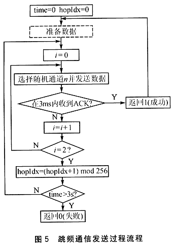
The sending process is shown in Figure 5. First initialize each parameter, and then select the transmission frequency point according to the pseudo-random number, and send data on this frequency point, and wait for 3 ms. If data is received, it means that the receiver is at the same frequency, and then data communication is performed on this frequency. If the timeout is 3 ms, try again; if the timeout continues, select the next communication frequency point according to the pseudo-random code to try again; if the timeout is 3 s, quit this sending process.
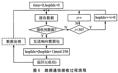
The receiving process is shown in Figure 6. The main loop is always in the listening state, and the receiving function is called cyclically. If a data packet is received, a response packet is sent. After the transmission is completed, hopIdx is incremented by 1, and the transceiver continues to monitor at another frequency. If no data is received at one frequency for a long time, it will switch to another frequency to continue monitoring.
This paper takes the half-duplex communication process as an example to introduce the realization process of anti-jamming frequency hopping communication. The programming environment implemented is uVisionII, and the test is passed under the Keil C51V7.08 compilation environment.
(1) Initialization process
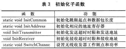
The initialization process mainly includes the setting of relevant parameters of the wireless transceiver, as listed in Table 3.
(2) Sending process
The main sub-functions included in the sending process are listed in Table 4.
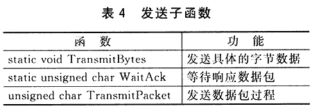
The main function of the sending process is implemented by TransmitPacket.
(3) Receiving process
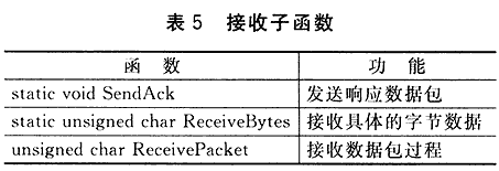
The main sub-functions included in the receiving process are listed in Table 5.
3 Summary
With the increasing shortage of wireless spectrum resources, it will become more and more important to adopt frequency hopping communication to realize anti-jamming communication; and using nRF9E5 to design and realize anti-jamming frequency hopping communication system is a cheap and convenient countermeasure, so it will be It has received more and more attention and application in the civilian market.
The Links: EL640201-U3 NL6448BC3370F

0 Comments for “The working principle and realization application design of anti-jamming slow frequency hopping communication system”