
It is reported that the Josephson junction is the cornerstone of superconductivity electronics and has good applications in precision measurement and quantum computing. Fabricating Josephson junctions is a resource-intensive, multi-step process involving photolithography and wet processing, which is incompatible with many applications.Therefore, researchers from Leiden University in the Netherlands invented a3D printingThe method of superconducting device using the Josephson junction effect.
Josephson junction (Josephson junction), or superconducting tunnel junction. It is generally a structure composed of two superconductors sandwiched by a very thin barrier layer (thickness ≤ Cooper electron pair coherence length), such as S (superconductor)-I (semiconductor or insulator)-S (superconductor) structure, Referred to as SIS. Superconducting electrons can pass through the semiconductor or insulator film from one side to the other side through the tunneling effect. However, in fact, as long as two pieces of weakly coupled superconductors (the size of the coupling region ≤ the coherence length of the Cooper electron pair) can form a Josephson junction, it does not necessarily need to be in the form of a tunnel junction. (From Baidu Encyclopedia)
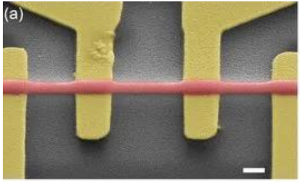
The Josephson effect occurs when the macroscopic quantum states are separated by a medium that allows their wave functions to partially overlap. This phenomenon occurs in the Josephson junction, where the macroscopic wave function of the superconducting electrode is coupled through some form of obstacle. Unlike traditional electronic devices, in traditional electronic devices, the current is driven by the potential difference (that is, the charge transfer in the Josephson junction is determined by the difference in the quantum mechanical phase of the superconducting electrode. The current phase relationship enables the Josephson junction to be lossless The efficiency of scattered transmission is combined with the accuracy of quantum interference measurement. Today, Josephson junctions are indispensable components in many fields, from high-sensitivity detectors for imaging and signal processing, to quantum circuits and superconducting calculations. For example, superconducting quantum interference devices (SQUIDs), also known as superconducting quantum interference devices, are very sensitive magnetometers. Such instruments operate by the Josephson effect and are widely used in science and engineering.
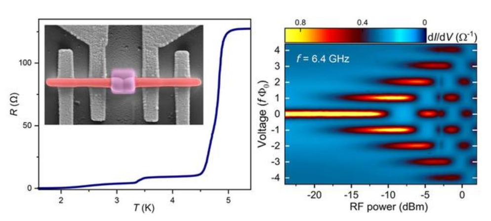
So far, the fabrication of Josephson devices has been a multi-step process. This is usually a combination of thin film deposition and other structuring/patterning steps, which can include photolithography processes (e.g. resist spin coating and etching) or exposure to a focused ion beam. These procedures are not always compatible with the potential applications of superconducting devices, for example, where fragile substrates or non-planar surfaces cannot be coated with resist, or when exposed to ion beams or immersed in liquids. When the system is harmful. There is no lossless direct writing method for manufacturing Josephson devices.
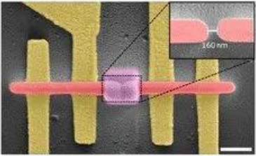
In this study, the researchers introduced a one-step addition technique to use electron beam induced deposition (EBID) to “print” the Josephson junction, that is, by scanning the electron beam to locally dissociate the precursor molecules, and then adsorb them on the surface. The entire manufacturing process is carried out in a scanning electron microscope (SEM) with a gas injection system, which can also directly carry out quality control and equipment maintenance. A complete Josephson knot can be printed in a few minutes. Except for contact with external electronic equipment, the EBID Josephson junction does not require thin film deposition or other treatments (such as annealing, exposure to chemicals or ion beams). This provides a non-invasive means to add high-sensitivity detectors, such as the superconducting quantum interference device (SQUID) for magnetic measurement, in the desired location of the existing structure.
0 Comments for “3D printed superconducting device invented by Leiden University in the Netherlands”