Microfluidic chip technology (Microfluidics) is the
biology
,Chemical,
medicine
The basic operation units such as sample preparation, reaction, separation, and detection in the analysis process are integrated into a transparent and reusable chip, and the analysis and operation are completed automatically. Microfluidic chips, as the main platform for the realization of microfluidic technology, are characterized by a micro-pipe network, which is at least one dimension of micron level (1~100 microns). The microfluidic chip has the characteristics of controllable liquid flow, minimal consumption of samples and reagents, and a high degree of automation. The whole process of processing and analysis is currently widely used in the field of life sciences.
The manufacture of microfluidic chips relies on microelectromechanical processing technology. The current mainstream processing technology is PDMS soft etching (Soft Lithography). This manufacturing process requires the use of photolithography to make a reverse mold in a clean room. The process requires a series of manual operations, and the high cost limits the structural complexity of the microfluidic chip, function expansion, and popularization and application.
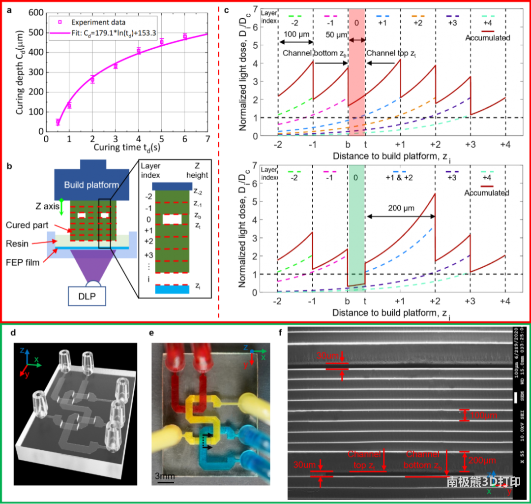
As an emerging microfluidic chip manufacturing technology, Vat Photopolymerization can realize one-step processing in ordinary environments, and easily print 3D pipe shapes with more complex structures, which is convenient for microfluidic technology research, promotion and sharing. .However, currently stereolithography3D printingThe microfluidic devices of 100% have difficulty achieving micron-level precision (less than 100 microns) along the printing direction. The root cause of this problem is over-curing in the printing direction, the Z direction. When printing the channel-roof layer and subsequent layers, it is difficult to ensure that the resin in the channel will not cure and block the channel.
02【Outline of Achievements】
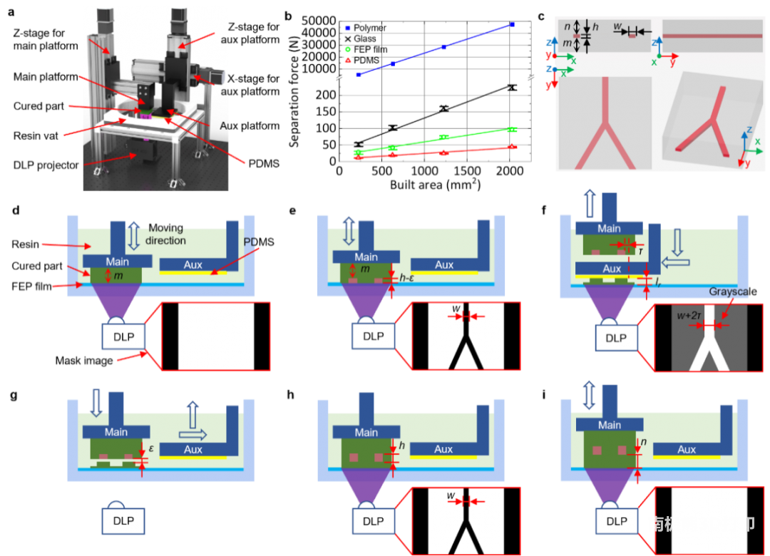
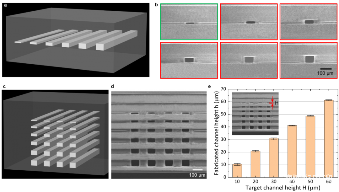
Professor Yong Chen of the University of Southern California and his team members Dr. Yang Xu (first author), and Professor Noah Malmstadt developed an in-situ transfer photocuring3D printingProcess (In-situ Transfer Vat Photopolymerization, IsT-VPP), this process can efficiently and reliably print microfluidic devices with a channel height of only 10 microns and an accuracy of ±1 micron, and has the potential to further improve the resolution of microfluidic channel heights Rate. The related research results were published in Nature Communications under the title of “In-situ transfer vat photopolymerization for transparent microfluidic device fabrication”. Other participants included Purdue University professor Huachao Mao, USC master students Fangjie Qi, Songwei Li, and others.
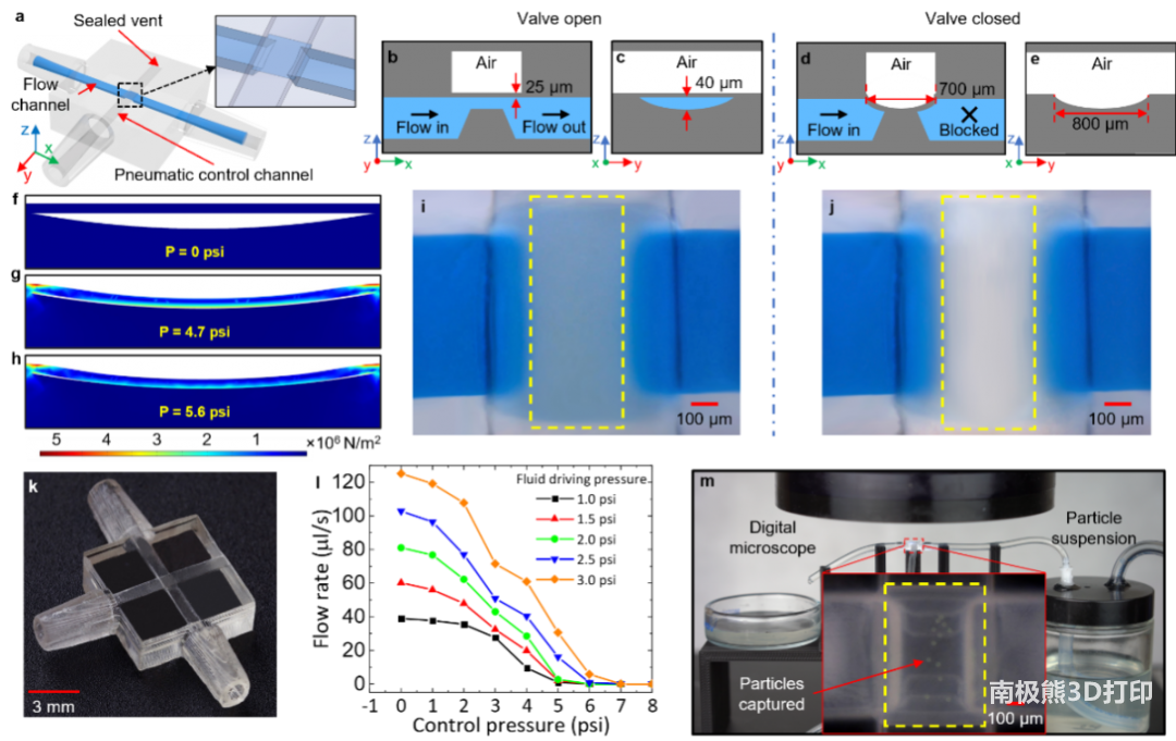
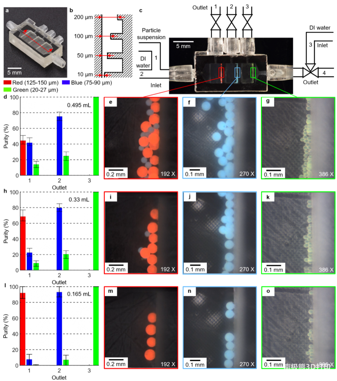
The core idea of this process is to add an auxiliary printing platform as a constraining plane on the basis of the traditional stereolithography printer, to print the crucial channel top layer separately through two exposures, and transfer it to the microfluidic device in situ. In this way, the light energy absorbed by the resin in the channel is greatly reduced, so that the total absorbed energy is much lower than the energy threshold required for curing, and the channel clogging caused by excessive curing is avoided. Using this method, the researchers printed a series of 10-micron-scale microfluidic channels and demonstrated a range of microfluidic applications, such as microfluidic valves, particle filters, and more.
03[Graphic and text guide]
04【Conclusion and Outlook】
Compared with other high-precision stereo light curing technologies, the experimental prototype shown in the article uses a low-cost 405nm light source and ordinary commercial transparent resin, without adding special light absorbers. In this way, the materials available for 3D printing microfluidic devices have been greatly expanded, and materials personnel can focus on developing new materials to meet biocompatibility and elasticity needs without worrying about printability. The researchers believe that with the help of high-resolution projectors or lasers, the precision of microfluidic devices 3D printed by the IsT-VPP process can be comparable to PDMS soft etching and the cost is lower, which will promote the development and application of new microfluidic devices.
Reference: Xu, Y., Qi, F., Mao, H. et al. In-situ transfer vat photopolymerization for transparent microfluidic device fabrication. Nat Commun 13, 918 (2022).
(responsible editor: admin)


0 Comments for “Blockbuster “Nature” sub-issue: New 3D printing process helps microfluidic chip manufacturing”