
FraunhoferFraunhofer Institute developed3D printingPiezoelectric MEMS micro-actuators are also inexpensive, which creates the economic production feasibility of piezoelectric MEMS in small batches.
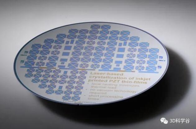
The technical structure of any geometric shape is applied to the wafer by inkjet printing and functionalized by laser radiation. The individual speaker components are then separated and integrated into the electronic environment. ©Fraunhofer ILT, Aachen
Paradigm shift of low-volume manufacturing technology
![]() Digital manufacturing improves stability
Digital manufacturing improves stability
According to the Science and Technology Information Center, piezoelectric MEMS can realize micro-execution, energy harvesting, sensing and wireless communication through a single chip, and it is a hot technology with great application potential. Piezoelectric MEMS micro-actuators can accurately and autonomously perform complex actions such as straight lines, rotations, accelerations, clamping movements, etc., so as to complete nano-scale precise operations on extremely small devices and structures.
Piezoelectric MEMS micro-actuators can not only meet the stringent requirements of integrated micro-systems (IMS) for self-testability, micro-positioning, and on-chip maneuverability, but also meet the output torque/volume efficiency ratio, response speed, and resolution of integrated micro-systems. Requirements in terms of efficiency, power consumption, and integration.
The Fraunhofer ISIT in Itzehoe, Germany, joined hands with the Fraunhofer ISIT in Aachen, Germany.Fraunhofer ILTDeveloped by the Fraunhofer Laser Institute3D printingPiezoelectric MEMS micro-actuator. This piezoelectric MEMS has six corners and is only about 1 cent in size.
This project is the result of a collaboration between the Fraunhofer Institute for Laser Technology ILT, the Institute of Electrical Engineering Materials (IWE2) of RWTH Aachen University and the Fraunhofer Institute for Silicon Technology ISIT. It is supported by the German Federal Ministry of Education and Research of the BMBF Part of the “GENERATOR of High-Efficiency Piezoelectric MEMS for Micro-actuators”.
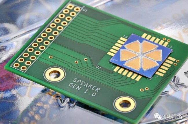 Hexagonal, slim and cheap. The micro-speaker jointly developed by RWTH Aachen University, Fraunhofer ILT, and Fraunhofer ISIT proves that using inkjet printers and lasers can produce micro-actuators in a few seconds at low prices. ©Fraunhofer ILT, Aachen
Piezoelectric MEMS are truly technical all-round products, because ultra-thin piezoelectric layers can perform both actuator functions and sensing functions: they expand when an electric field is applied, or convert mechanical motion into voltage. Therefore, they are magical in communication or medical technology, for example, as sensors or actuators in pumps, valves, or speakers.
Piezoelectric MEMS films are usually made of lead zirconate titanate (PZT), which is currently the most powerful piezoelectric functional ceramic. Piezoelectric layers with a thickness of a few μm can be constructed very precisely by etching or direct printing.
![]() Laser-assisted printing process can replace traditional high vacuum coating
Laser-assisted printing process can replace traditional high vacuum coating
So far, the production of piezoelectric MEMS has used traditional vacuum and mask-based manufacturing methods, but these methods are very time-consuming and costly, especially in small-batch production.
As part of the GENERATOR project funded by the German Federal Ministry of Education and Research (BMBF), the Fraunhoer Laser Institute Fraunhoer ILT, the RWTH Aachen University, and the Fraunhofer ISIT Silicon Institute jointly developed the digital inkjet The process combination of printing and laser crystallization has become a favorable alternative to traditional manufacturing processes.
After applying the PZT lead zirconate titanate special ink to an 8-inch silicon wafer, it is crystallized by laser radiation with a local temperature exceeding 700°C, and the quality is ensured by a temperature-controlled laser beam. The temperature control process can limit temperature fluctuations within ±5°C.
![]() Multi-material stacking trend
Multi-material stacking trend
Several thin PZT zirconate titanate layers of 20 to 30 nm form a multilayer actuator with a total thickness of 2 to 3 µm. According to the further understanding of 3D Science Valley, the scientists initially only applied a single layer, and then tried to create a multi-material stack layer by layer, and finally realized a complex structure with up to 30 layers of functional ceramics and electrodes stacked on top of each other.
Thanks to this design, the additive-manufactured actuator has better performance and higher reproduction quality than conventional actuators. The PZT layer and the electrode layer are interlocked like two very thin combs. The rapid laser processing of the layers reduces the processing time of each layer by a few seconds, while the processing time that would otherwise take several minutes is only a few seconds.
In addition, in order to replace ordinary and very expensive platinum, scientists use conductive ceramic lanthanum nickel oxide (LNO) as the electrode material. By eliminating metal parts, the durability of these pure ceramic multi-material laminates can be significantly improved while reducing material costs.
If an AC voltage is now applied to this multi-material stack, the PZT layer will deform within a fraction of a second, thereby exciting the entire stack to vibrate. Since the entire system is only a few microns thick, it is possible to transmit sound signals excellently in this way, especially in the high frequency range.
The advantage of this manufacturing method lies in the digitally controllable printing and laser processes that allow immediate design changes to the manufactured layers without the need to pay additional costs for masks or tools, so that small batches of products can also be produced.
This manufacturing method opens up development opportunities for small and medium-sized enterprises to enter high-end thin-film electronics. 3D Science Valley understands that conventional systems used to manufacture thin-film electronics cost millions of euros, so it is only worthwhile for mass production. For smaller batches, the additive manufacturing process becomes interesting, especially when the component is composed of several layers such as micro speakers.
Therefore, the Fraunhofer Institute developed3D printingPiezoelectric MEMS microactuators are particularly suitable for small and medium-sized enterprises, because the investment in system technology is significantly cheaper than conventional technology. Users need proper printing and laser system technology, as well as specially modified PZT and LNO inks. Even small workplaces can build small-scale production of micro-actuators in the future.
So far, this method has used coating silicon substrates. After setting up multiple stacking systems, these substrates still have to undergo relatively complicated post-processing to produce usable components. However, the nature of the laser-based manufacturing process means that other substrates (such as ultra-thin glass) can also be considered, which will further simplify production and open up a wide range of possible applications.
In the course of this project, in addition to process development, 3D Science Valley learned that scientists can also produce exciting results on the basic mechanism of laser crystallization of ceramics in the millisecond range. There are new possibilities that arouse great interest. Perhaps it will soon be transferred to other materials and thus to other applications.
![]() Manufacturing and innovation are coupled with each other
Manufacturing and innovation are coupled with each other
The book “Seven Secrets of Germany” points out that Fraunhofer couples manufacturing and innovation, and the United States has no institution that can rival Fraunhofer. The Fraunhofer Institute focuses on applied research, with the goal of providing solutions with commercial value, and building a bridge between basic research and commercialization.
(Editor in charge: admin)
0 Comments for “milestone! Fraunhofer develops 3D printed piezoelectric MEMS microactuators”