
Additive Manufacturing System Suppliers As mmWave Electronics Market Grows
Optomec
Introduced a new high-performance semiconductor packaging solution for 5G, autonomous vehicles, defense and
medical
needs of users in the field. Millimeter-wave integrated circuit (IC) applications are growing at a compound annual growth rate of 27%, but are still difficult to achieve widespread adoption due to traditional techniques for connecting ICs to circuits that degrade circuit performance, such as low wireless range and/or high power consumption . Optomec3D printing3D Printed Interconnect solutions address this issue, maintaining device performance through low-loss connections.
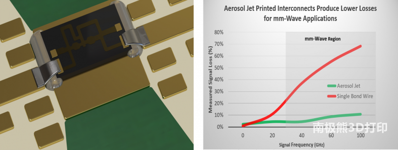
Optomec customers report doubling the transmitted signal power per circuit connection in the millimeter range, enabling longer point-to-point range and lower energy consumption for wireless data transmission. And because low-power ICs can operate at lower temperatures, ICs last longer. This mmWave band covers 30 to 300 GHz.Typical wireless networks in the home or office today operate at 5 GHz, and next-generation wireless mmWave networks will operate at frequencies up to 53 GHz; automotive radar, defense applications and
medicine
Imaging sensors operate at even higher frequencies. Older methods of connecting ICs, such as using tiny gold wires, became less effective as frequencies continued to increase, but Aerosol Jet® printed IC connections was more efficient, with performance almost comparable to etching the copper traces of a circuit board.
Bryan Germann, Product Manager at Optomec, said: “Our customers have also described some excellent performance improvements in mmWave interconnects. Many industry customers using mmWave frequency bands have learned that printing interconnects instead of
standard
The benefits of wire or ribbon bonding. Shorter and better impedance matching transitions can reduce losses per chip-to-chip, or chip-to-board transition, improving overall device efficiency and performance. “
The Aerosol Jet™ process works by jetting extremely fine droplets of nanoparticle conductive ink onto circuit boards and components within 10 mm, producing conductive particles with a width of 10 microns. With ultra-high print resolution and integrated vision-based alignment, Optomec’s new Aerosol Jet™ HD2 printer is optimized to support this new IC solution for complete production applications. The HD2 supports standardized in-line automation and can be integrated directly into existing packaging lines. Optomec also further provides customers with a library of pre-certified print recipes and applications to provide a total solution ready for production.
(responsible editor: admin)
0 Comments for “Optomec Introduces High-Performance Semiconductor Package 3D Printed Interconnect Solution, Doubles 5G Signaling”