
Writing information and erasing handwriting on paper is commonplace. Whether it is a child who is just learning to write or a researcher in the field of science, writing and erasing on paper is a daily routine in life. Pencil writing is easy to erase, but pen writing is not easy to erase.Similar to this, all the rage3D printingThe technology also has a pain point, that is, how can the printed structure “erase” the unwanted parts with high resolution? Let’s look at the field of chemistry again. The reversible formation and breaking of covalent or non-covalent bonds in reactions can also be broadly regarded as “writing” and “erasing”.So, is it possible to introduce the formation and breaking of chemical bonds to3D printingTechnology to realize the reversible “erasing” of the printing structure?
Recently, Karlsruhe Institute of Technology (KIT) Martin Wegener, Christopher Barner-Kowollik, Eva Blasco, etc. took the photosensitive polymer system as the starting point for their research and adopted photoresist resins containing o-nitrobenzyl ether (ONB) conduct3D printingResearch on optical writing and erasing of microstructures. Based on the 900 nm light-induced free radical polymerization and crosslinking of acrylate monomers with the aid of photoinitiators, and the photodegradation of ONB functional groups under 700 nm laser irradiation, the research team achieved a fine 3D structure through light control at the same time for the first time Construction and selective erasure. Related papers were published in Advanced Materials.
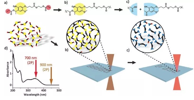
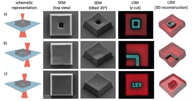
In order to avoid the photodegradation of ONB group caused by light in the process of acrylic resin photo-initiated polymerization, the research team determined that the femtosecond laser has a wavelength of 900 nm and a power of 8 mW through screening.3D printingThe optical writing rate is 100 μm s-1; the laser erasing wavelength is 700 nm, the average power is 10 mW, and the solvent system is DMSO.The research team uses the above-mentioned 900 nm wavelength laser3D printing15 × 15 × 5 μm3 cube structure, followed by a 700 nm wavelength laser to selectively erase the cube structure, and finally obtain a variety of complex 3D structure devices. The SEM test shows that the microstructure morphology formed by optical erasure has smooth edge structure and good spatial regularity, and has excellent practicability in the preparation of complex microstructure 3D structure devices such as microfluidic devices.
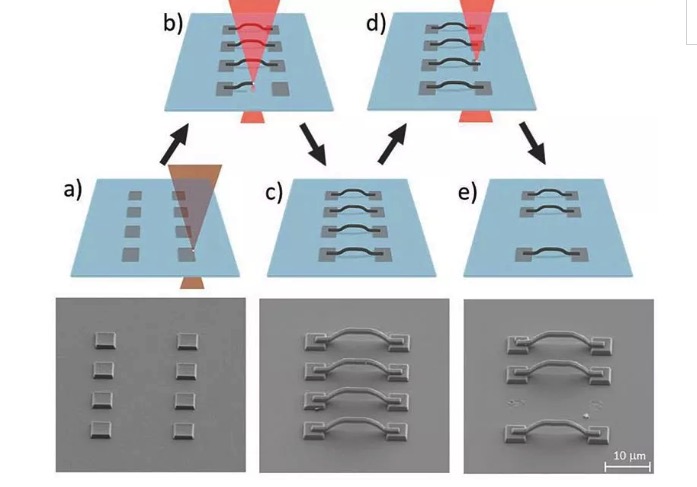
To further demonstrate the compatibility of the ONB-containing photoresist resin with commercial photoresist resins, the researchers used ONB-containing photoresist3D printingPrepare a 5 × 5 μm2 square base, and use commercial acrylic as the material to prepare a linear connecting member between the bases. Based on the remaining reactive functional groups in the ONB-containing resin matrix, the base resin can form a covalent bond with the linear resin. Based on the 700 nm light erasability of the ONB resin base, partial individual devices in the 3D microstructure array can be completely erased through selective exposure.
Summarize
Photoresist’s unique photo-crosslinking or photo-degradation properties make it widely used in the field of microstructure preparation.This paper introduces both photocrosslinking and photodegradation functional groups into the photoresist resin at the same time, with the help of advanced3D printingThe simple molding technology realizes the construction of various complex 3D microstructure devices and the secondary local structure control of the molded devices. At the same time, the excellent compatibility of the new photosensitive resin and commercial photoresist in the research results gives it a unique advantage in the preparation of composite microstructure devices.
(Editor in charge: admin)
0 Comments for “Researchers develop erasable new photosensitive resin 3D printing structure”